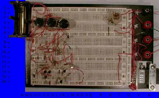
Also I have borrowed a couple of photos from another website, and I am awaiting permission to use them. Until you see this language removed please consider the combined front, and back views of the proto board to be exempt from provisions of the Design Science License until such time as I get permission to use them, and point a link to their site.
If you are a student of my webpage I welcome you, but please keep this notice in mind, and plan on re-reading this unit when this notice goes away, as that is your signal that I consider it to be in finished form.
Here I try to show you transistor configurations that yield performance advantages that are targeted to specific problem areas, and intended to eliminate tradeoffs in the simpler basic transistor configurations, I introduced in lesson 017. If you feel the least bit uncertain about how the basic transistor configurations work, or failed to grasp concepts such as what a pull up resistor is for, why inversion is only associated with common emitter, and not common base, or common collector, you need to puzzel over these things, until you get it. I did not tell you why inversion only works in common emitter circuits. I do not intend to explain that. If you grok the three amplifier circuits you should know the answer to that question. If you don't know, you didn't get it. I'm not trying to be hard on you, but if you proceed into this lesson failing to understand these most basic precepts you will be lost.
Click the "Audio discussion"
link now, then read on while
it's downloading.  When it
arrives, come back here to
view this circuit diagram as
I explain how it works.
Also:
Please read this whole lesson before going out to buy parts. I have designed these experiments with the idea in mind that many of you already have workable alternatives on hand. Indeed if you are really well stocked you won't need to make a trip to the electronic surplus store at all, if you consider the alternative component selection guidelines given later in this lesson, immediately after I call out the component values of the Discreet Operational Amplifier
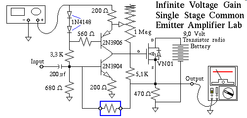
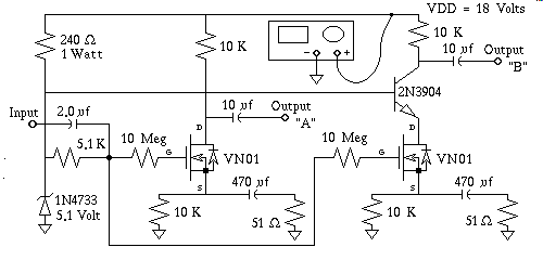
In the above circuit I introduce a new device, the VN01 is a rather generic part number for an Enhancement mode "N" Channel MOSFET the symbol for the MOSFET includes the protection diode that is connected between the source and drain terminals internally to the part. The Source lead is the one on the bottom and it is marked in this diagram with the letter "S", the Drain wire, and marked with a "D", and the third wire marked with a "G" is the Gate lead. In the current configuration the MOSFET is wired up as a Source Follower and it is similar to an emitter follower in function, with one big difference. The Gate lead unlike its Emitter Follower cousin's base lead, subjects the transistor circuit to no load what so ever. This is because the Gate lead connects to an electrostatic field based device, that is totally electrically insulated from the source/drain portions of the silicon chip. The agent that is providing the insulation is a thin layer of metal oxide. The term MOSFET, is an acronym, that means, Metal Oxide Semiconductor, Field Effect Transistor. In lesson 016 I explain how a vacuum tube diode works, and then I go on to show what happens if you place a grid wire between the filament, and plate. I point out that this triode (three electrode) tube produces an amplifier, by setting up an electric field that controls the flow of electrons between the filament, and plate. In this sense FETs are very similar to vacuum tubes. In fact common Junction FETs work, ignoring their bidirectional nature, exactly like vacuum tubes. In a common junction FET the junction is reversed biased setting up a large depletion zone. The larger the zone, the less cross sectional area of the source and drain portion of the crystal is available to carry electrons, and the size of the depletion zone, is a direct result of the reverse bias of the junction, that forms the gate of the FET. Thus something that draws no current is controlling a sizable amount of current somewhere else. I do not intend this to be any more than an introduction to FETs at this stage of the course. Although in the interest of completeness I will say that Enhancement Mode is accomplished by using a dopant structure just below the metal oxide layer, that has the effect of making the zero bias voltage of a FET more like a transistor than a vacuum tube, in that an Enhancement mode MOSFET is normally open, that is, its zero bias condition makes it turn off, as opposed to it's Depletion Mode counterpart, which behaves more like a common Junction FET eg. normally on, conducting at zero bias. In closing this brief intro on MOSFETs, it is very important to stress that the gate of a MOSFET is truly insulated, it will easily accept static electrical charges sufficient to permanently destroy the device. While you are working with a MOSFET do something to connect the Gate, and Source lead wires together until you have it installed into the circuit. Just sliding your hand across the table can generate voltages that are destructive to a FET, or MOSFET.
The Current Source:
The two 1N4148 diodes form a negative reference voltage of 1.4 volts with respect to the positive main supply, coming from in this case your homebrew bench supply that you built in the previous lesson. This of course doesn't work unless the bench supply is producing at least a couple of volts, but as soon as you dial it above the point where these two diodes forward bias they produce a nice regulated bias voltage for the 2N3906 PNP transistor. This transistor if safely out of saturation, will as a result of emitter voltage of 0.7 volts dropped across the top 300 ohm resistor produce a collector current of 3.5 ma regardless of the collector voltage.
The Common Emitter Amp:
The 1N4148 diodes the 3.3K ohm, and the 680 ohm at a bench supply of approximately 10 volts bias the bottom transistor such that it too is feeding a collector current of 3.5 ma back toward the current source. If you remember my saying from the previous lesson's discussion on the voltage gain of a common emitter amplifier is the ratio of the total impedance of the collector circuit, divided by the total impedance of the emitter circuit. Since in this circuit the common emitter's collector impedance is determined by a current source for a pull up, and the insulated gate of a MOSFET, the total collector impedance is theoretically infinity. So voltage gain is infinity divided by two hundred ohms, the emitter impedance, equals infinity. Crazy math but that really is what it means.
In practice losses in the system generally make the simplistic current source used here not so perfect as we would really like, what to do... what to do... As it turns out you can tease that last ounce of performance out of this circuit by using just a smidgen of positive feedback to offset the miniscule imperfections. This is the purpose of the 5 meg ohm potentiometer.
I want you to build this circuit, and make it do what it does, it teaches positive, and negative feedback, what constant current is, and many other things. I expect you to build it, but you need to fill in a couple of areas first. Potentiometers need not be made linear, after all the manufacturer determines what material to use for the resistance element, and the wiper arm. Indeed they control every facet of its manufacture, if it were advantageous to make the pot so that it required ten full rotations lock to lock, and they believed that customers would pay extra for such a thing I'm sure they would figure out a way to make them. Well guess what, a pot that requires ten full rotations lock to lock, allows you to adjust the pot to very precise resistance settings, without requiring you to have the steady unflinching hand of a Swiss watchmaker. So the manufacturers of potentiometers have devised several methods of producing multiturn pots. The best, and most expensive involves winding very fine resistance wire, usually an alloy called Nichrome about the diameter of human hair onto large diameter, (about the size of a pencil lead) enameled copper wire, the stuff you normally wind coils, and electro-magnets with. The enameled copper wire simply serves as an insulated coil form on which to wind the super fine resistance wire. No electrical connection is made to the large diameter enameled copper magnet wire. Then they coil that heavy gauge wire, with the fine resistance wire wound onto it, into a one inch cylinder, and place it inside of a larger cylindrical plastic body, that has a mechanical assembly, that causes the wiper arm to track the helically wound resistance element, such that you can dial in multiple turns, and what happens inside the pot is the wiper arm is screwing its way down the length of the cylinder. If you had chosen to use this kind of pot for the front panel of your bench supply it would allow you much more precise control.
Likewise the resistance material they use need not be uniform. They can, and do make pots that the resistance change at one end of the knob for a given percent of full rotation, is different at one end of the dial, than for the other. In fact this nonlinearity can follow transcendental function curves. One of the most common is to have the resistance be an exponential of the angular knob rotation. Pots that have this characteristic are called Logarithmic Tapered or Audio Tapered pots. While pots with a uniform change in resistance per unit angular rotation are called Linear Tapered pots. The feedback pot, is, for any range of resistance more likely to provide better angular knob to feedback resolution if a Logarithmic Taper is used rather than the more conventional Linear Taper pot. Using a pot with a nonlinear taper requires you to pay attention to which ends of the pot have the most / least delta-R versus delta-A ratios. In our specific case using an audio taper pot the low delta-R, should also be the low resistance side of the pot, and the high delta-R is the high resistance end of the pot in order that we may take advantage of the taper an audio pot provides. An audio taper pot, has low delta-R at the CCW, Counter ClockWise end of the rotation, so that will be where we connect the wires.
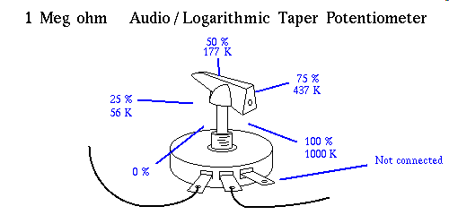
Get out your scientific calculator and I'll show you. Pick any number from 2 to 9 and subtract a small but consistent number from it. Say 0.1 for example, and add that same small constant to the number you first picked. You now have three numbers, a high, a medium, and a low number. Take the exponential of the high number, and then subtract from it the exponential of the low number. Then take the result of that subtraction, and divide it by the exponential of the medium number. If you used 0.1 for the delta-A (change in angle) your answer will always be 0.464597 no matter what number you pick to start your calculations, assuming you used 10 to the x and you used plus, and minus 0.1 for delta-A. By making the resistance exponential to the angle of rotation causes the angular resolution of any given delta-A on the potentiometer to always be the same resistance resolution, delta-R to total-R ratio, no matter where the knob is pointing on the dial. Note: if you used some other value than 0.1 for an angular delta, your answer will be different, but using your same chosen delta-A at numerous points on the curve gives the same result every time you run the numbers. Likewise if you used e to the x and still used plus, and minus 0.1 as your deviation delta, your answer would always be 0.2003335
Ok this is pretty amazing, but why do they make an audio volume control knob follow the logarithmic curve? The answer to that question opens up a whole new and exciting field of study. Your ears hear ratio metrically, with respect to change in loudness, as it is referenced to loudness as a whole. This means many things, one significant item is that you are unable to detect with certainty, anything less than a two to one speaker power level change in isolation from other sound. Audio engineers have developed the Bell scale to quantify this. To be more specific, or perhaps more familiar, the scale is then subdivided further into ten equal parts, we call these divisions Decibels and the decibel scale is logarithmic, therefore to accurately and uniformly place division marks on the dial of a volume knob, because of the nature of human ears being logarithmic, and the division marks on the dial being linear, the potentiometer used for volume control has its resistance element manufactured with an exponential curve with respect to angular rotation. Another way to say the same thing is to state the audio volume control pot has its angular rotation logarithmically skewed with respect to its resistance. Often the marks on a Volume Knob are calibrated in either 3.0 db intervals, or 1.5 db intervals, depending on whither they placed ten or twenty division marks on the dial the knob of potentiometer points to. This decibel rating is a power rating, where 3.0 db represents a two to one power increase / decrease, ratio depending on the sign of the decibel number, or a square root of two to one voltage increase / decrease, ratio again sign dependent. This 3.0 db figure is magic, because 3.0 db is the point where power doubles, and since the knobs angular rotation is Logarithmic with respect to the actual resistance, hence voltage / resistance ratio. If the marks on the volume dial are spaced evenly at 3.0 db intervals each mark represents the minimum volume change the human ear can detect. This is terribly subjective, frequency dependent, and ruled by psychoacoustics.
I digress:
I probably shouldn't spend the time here, but this has opened up an interesting phenomenon, that you really should know about. Any point source of radiant energy, and a sound source belongs in this discussion as you will come to understand, behaves according to the Inverse Square Law. Since you are not accustom to seeing sound waves, I will use visible light to make the point.
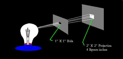
What does this say about the intensity of the light, at the point that it impinges on the second plate. The amount of light allowed to pass through the one inch square hole of the first plate remains the same, since we did not move it. Since the light is a fixed quantity, the light that falls on the target must also be that same sum total. However now the light is spread out over nine square inches. therefore the light that falls on any given square inch of the target, is one ninth the original total. Therefore Light intensity ratio is one, divided by the square of the distance ratio.
            1
Li = ---------------
      distance^2
This is called the inverse square law, and it comes up over and over again
throughout the discipline. We see it explaining how much radio energy will
fall on a receiver's antenna, based on how far away the receiver is from
the transmitter site, and how powerful the transmitter is. Turn this
argument around we can figure out just how powerful we need to build the
radio station to reach a radio, at the distance we wish to cover, and still
be able to deliver enough radio signal to create a reasonable signal to
noise ratio.Sound is generally a point source, omni directional phenomenon, rather like the lamp, and as you step away from the loudspeaker, the level of energy that vibrates your eardrums, follows the inverse square law. Your mind is playing many psychoacoustic tricks on you, one of which is making the sound appear to change more in line with linear phenomenon, than with the square of the distance. This stuff is very involved, and if you are interested in psychoacoustic phenomenon, you might take a gander at my asdf-0.4.tgz in the files section of this web site. It is a very simple audio compression system. There are much much better ones out there, but a simple one is easier to understand when you are first starting out.
Anyway, back to sound ratios, if you change your distance by the square root of the ratio 2:1 normally pronounced "two to one" you will in effect create a power level ratio of 2:1 that is you will either halve, or double the power level of the sound impinging on your eardrums, depending on whither you backed away from, or advanced toward the loudspeaker. I mention this, because the next statement will make you see just how seriously psychoacoustics is interfering with your perception of the relative intensities of sound. Listen carefully: Standing ten feet from the loudspeaker, if you step backward four more feet, sound intensity is half the energy, level, eg. power, or watts! If that doesn't grab you, you're not thinking about what this means. Close your eyes and try to imagine what music playing from a radio, standing ten feet away sounds like, and then again after backing away four more feet. You've done this many times, do you remember the sound level being anywhere near half? Unless you come from my home planet, you are human, and human perception, and psychoacoustics being what they are, makes this change in distance appear to the human ear, considerably less than a two to one change in power level. Think about it and you will see what I mean. Ok now that I have forced that paradigm shift, I will now proceed to blow your mind again. Guess what else is affected by this perception phenomenon... Practically every sense you have, be it sight, hearing, pain, smell, taste, touch, heat, cold, time, electrical shock, electrical muscle stimulus, radio frequency stimulus, tensel feedback, and vocal feedback are all processed in the brain, and reassigned severity values in such a way that all these senses can be interpreted as one harmonious single unit. On the home planet we never evolved a mechanism that makes sound appear louder when the lights go off, living with two suns prevented that characteristic from ever evolving in us, but as I understand it humans do experience this effect, and for some it is quite noticeable, it is in part why small children are so afraid of the dark.
If you're unsure of this, I call upon you to take the Common Log of 2.0 eg. power doubling, and then take the Common Log of 0.5 eg. power cut in half, the first result is 0.30 Bells or in layperson speak 3.0 decibels the second result is negative 0.30 Bells or in layperson speak minus 3.0 decibels. Oh and why is the Voltage decibel number half the Power decibel number? Well if you remember the Ohms Law Pie Chart in lesson "009 Confusion solution" Power at a given, in this case speaker impedance, is a Voltage Squared function, and since multiplying Logarithms had the effect of raising the exponential result to that power, Doubling the Voltage Decibels, computes Power, by effectively squaring the number by the time it gets to the exponentially curved resistance element. This stuff is wonderful to understand and use, but try imagine for a moment, what thought processes must have been involved to invent all of this, and you start to gain a real respect for the giants whose shoulders you are now standing on. Those of you familiar with the operation of a slide rule will already have direct experience in this area. A slide rule is nothing more than various logarithmic scales applied to the problem of solving multiplication / division, exponents / logs, and powers / roots by method of the linear addition of these logarithmic scales by literally sliding these ruled scales against one another, to gain a mechanical offset. My goal is not to present you with training for an abacus, when you have a computer sitting in front of you, however, a Slide Rule teaches many principles, learning to use one can broaden your understanding of math substantially, if you are ever in the position to learn the use of one, don't turn down that opportunity, it can be very enriching.
Teasing the bias threshold:
This subject is covered, in exquisite, and excruciating detail in the open mic audio discussion. You should play the audio back now, and then once again when you have the experiment set up, and ready to perform.
Teasing the bias:
Noise Happens, Ok: I didn't invent noise, we generally don't want noise, but it's all around us. It is part of this thing we call analog. If you break the positive feedback circuit, that is, you open either wire of the 1 meg ohm pot, your circuit will, as you turn up the voltage on your bench supply past 3 volts begin to reflect this change in the output voltage measured at the source of the FET. At the point you reach about 10 volts, any further increase in bench supply voltage produces a drastic reversal in the output, that is, the voltage once it reaches some maximum rapidly collapses to zero. If you tease the bench power supply just exactly right you can get the output voltage to ride at about half way between it's maximum, and zero. This is for our purposes the "Q" point, or Quiescent Point. Get a feel for this, play with it by teasing the knob to see how much freedom of rotation you have, but remain in the grey zone, between max voltage, and zero, yet still in the inversion zone, where increasing bench supply voltage produces diminishing output voltage. Now reconnect the 1 meg positive feedback pot, predialed to maximum resistance FIRST before you reconnect. Now go back and forth, first teasing the knob on the bench supply, then trying to reduce the resistance of the the 1 meg positive feedback pot, a little bit at a time. Eventually you will find the sweet spot, the point at which the gain goes so high that you cannot get the circuit to completely stabilize, because the ambient noise of the circuit is so great with this incredibly high gain that it interferes with your efforts at biasing for the "Q" point. If you are watching this on an oscilloscope, you may even see it breaking into oscillation at these incredibly levels of gain. Reducing the 1 meg positive feedback pot's, resistance further, causes the amplifier to Regenerate that is in this case DC regenerate. When total positive feedback of such a system, exceeds total negative feedback Regeneration is the result.
The same thing stated another way is,
"when total loop gain exceeds unity gain Regeneration occurs"

Where:

total loop gain   = the product of all gain, and attenuation.

unity gain        = 1.0 by definition, eg. no gain at all
Negative feedback:
I will assume you have successfully squeezed all the voltage gain that can be achieved with this primitive circuit. I now direct your attention to the unmarked resistor outlined in a blue rectangular box. This resistor sets the Negative Feedback of the circuit. If an amplifier truly has infinite voltage gain, a negative feedback such as this, for the moment we will dispense with the AC effects on the base circuit impedance the 3.3 K, and 680 ohm resistors cause, and focus only on what the feedback resistor is doing to this circuit. Although no amplifier can ever truly reach infinite voltage gain, for various reasons, among them noise, and stability make it impossible to even detect that you have infinite gain, even if you in fact, do. That aside we will assume that your gain is high enough that what I am about to state, is still for the most part, true, and verifiable. For any reasonable negative feedback resistor, say for starting point 10.0 K ohm the input impedance so long as the Common Emitter amplifier transistor, and the Source Follower MOSFET are neither Saturated, or in Cutoff the input impedance is ignoring the Xc eg. capacitive reactance of the front end AC coupling, or DC blocking capacitor, is for all purposes zero ohms.
I'll now restate that without all the qualifiers. The input impedance of this amp is a direct AC short circuit!
Any generator you connect to this amp has at least some internal impedance, albeit low, it's still there, so when you connect it to this amp whose input appears to anything connected to it as an AC dead short, a current flows, throughout the generator, and into the amp, but oddly not into the transistors base? What is happening here? The open loop gain is so incredibly high, that the feedback is carrying all of the AC current fed in from the generator. Huh? I hear you say how is this possible? In a negative feedback circuit with a sufficiently high open loop gain amplifier the Output will do what ever it has to do to completely null out the input current! The profound effect here is that such an arrangement has a zero impedance input, and a voltage output. Put another way this input is current sensitive, not voltage sensitive, you can't put voltage across a short. So this is a current to voltage converting amplifier. This has a name, we call these circuits Norton amplifiers. This type of amplifier has many uses, I will mention two.
Magnetic Tape Heads, and magnetic pickups in phono styluses, and the like are coils. Coils by their very nature are inductive. The lower the impedance you drive an inductive pickup into, the longer it holds its magnetic field. If you want to greatly extend the low end frequency response you drive the output of your magnetic pickup into this type of an amplifier, one that achieves zero input impedance via negative feedback.
Junction FETs are bidirectional AC resistors controlled by a reverse biased gate that chokes off the flow of current in both directions between the Source and Drain at ever greater ferocity the higher the reverse charge. By choking off the flow of current, I mean what it does is to effectively reduce the cross sectional area to almost nothing at high reverse bias. What this choking accomplishes is to alter the resistance of the single "P" or "N" type material. Such a device is a natural for building a Gain Controlled amplifier, except for one small detail, that tends to derail the whole thing. The voltage that does the "controlling" is referenced to some undetermined midpoint in the semiconductor crystal as a whole. So if we send AC signal across the crystal, some of that signal is present as a reference to the Gate junction. This creates Logarithmic distortion in much the same way the Common Emitter amplifier did in lesson 017, the previous lesson. By using a nearly zero impedance amplifier we also guarantee that the AC voltage will be virtually zero across the input terminals of the amplifier. If the Source and Drain of the FET is wired across such an amplifiers input terminals the logarithmic distortion introduced will be practically nonexistent. If the gain were actually infinity, the input impedance of the amplifiers input would really be zero, so any parallel connected FET would have no effect what ever. You see zero in parallel with any resistance is still zero, eg. no change. In truth you really can never attain infinite gain, or zero input impedance, but getting close, allows the FET to control the overall gain by shunting a very small input impedance, while keeping the AC voltage low enough that it doesn't cause logarithmic distortion severe enough to be detectable.
The Discreet Operational Amplifier:
The previous single stage infinite gain amp, was not a practical amplifier because it required an operator to "tease" the bias into operation. The following Amplifier is practical, although it seriously suffers from a poor high frequency response, called, Gain Bandwidth Product. This circuit is in fact a discreetly wired Operational Amplifier. Because we have used no capacitors, and no inductors, this circuit could be theoretically built into an IC, (integrated circuit), in other words we could, if we had enough money, build it on a silicon chip. So why not just use an IC Op-Amp to begin with? By approaching the subject this way, you get real hands on experience with the inner workings of such a circuit. Remember my calling out biasing limits, and voltage limits of the inputs. As a discreet transistor circuit I can address such things directly, rather than instructing you to simply take my word for it. You will come to understand how the inside of this Op-Amp actually works, rather than some lame coverage that leaves holes in your understanding. If you haven't guessed I expect you to build this one too.
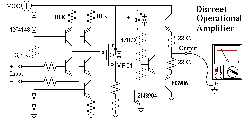
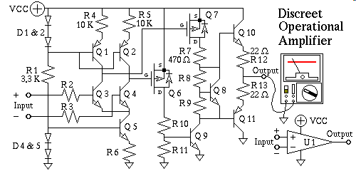
In general using 5.1 K ohm for most of the resistors is not critical that they be 5.1 K ohm, you could use some other nearby value such as 3.9, 4.7, 5.6, or even 6.2 K ohms if some care is given to their ratio dependent counterpart. For example if you have a good supply of 4.7 K ohm resistors but lack any 5.1 K ohm resistors in your parts drawer, you could use them instead, but you should cross multiply to maintain the same ratio of current in the two resistors in the pull up current sources. To be specific, R4, and R5, should be a little lower as well, I would change them from 10K to 9.1K if I were using 4.7K resistors in place of 5.1K throughout the circuit, only because of the current balance at the zero offset condition of the differential input transistors Q3, and Q4 we would really like to preserve a true balance of the pull up, Q1, and Q2 current between the pull down current sources, in this case Q5. The zero offset condition of the differential input is the critical point at which the current switches from one side to the other, causing the "P" channel MOSFETS to divert current from one to the other, ultimately causing the drain of Q7, and the collector of Q9 to to place a change of voltage at the input of the Q10, Q11 voltage follower pair. The reason we need this ratio preserved is that we really would like a make before break action in the gates of Q6, and Q7 differential voltage detector / translator pair. Another such ratio, that's very important to the circuit as a whole is that of R8, and R9, these are important because Q8 is providing bias voltage to the voltage follower circuit, if the ratio of R8, and R9 is incorrect, the voltage follower will be under, or over biased. Over biased is really bad because it causes Q10, and Q11 to fight each other thus dissipating enormous amounts of heat, and ultimately self destructing. If you understand these guidelines, you can probably make these kind of substitutions on the previous experiment, the Infinite Gain Amp, in it there is rather less room for these types of mass substitutions, all though I will point out a couple of areas. The 3.3 K and the 680 ohm, produce 1.4 volts when the bench supply is at 10 volts. If you change those, and maintain the ratios, thats ok if you stay within 15% of the base value, but also the 560 ohm, is attempting to maintain a thevenin impedance on the base of the 2N3906 that is equal to the thevenin impedance, open loop, of the 2N3904. The 200 ohm emitter resistors, if changed should be the same value in both emitter resistors to keep the currents balanced as well. In changing these I would caution you not to go below 180 ohm, or above 240 ohm as this experiment pushes the limits of what a single stage common emitter amp can do. A lot of effort was spent to insure that this experiment would work on your bench using garden variety components. If you experience symptoms such as DC regeneration with the 1 meg pot dialed wide open, you probably have made a poor choice in a substitution somewhere, or possibly a simple wiring error.
Q1 and Q2 are pull up current sources not unlike the 2N3906 transistor in the Infinite Voltage Gain Single Stage Common Emitter Amp Lab at the start of this lesson. If you built that circuit you have a feel that words cannot convey for the kind of behavior two current sources fighting each other exhibit. I can tell you that division by zero is meaningless, but in the absents of anything real to connect such a fact to, the words have no impact on you. With a pull up resistor in the common emitter circuit, ohms law works, and the computation of gain has meaning. Trying to wrestle with things like predicting the voltage of a transistor under bias with a pull up resistor in the collector circuit is a simple matter of applying ohms law. But a pull up current in the collector circuit, now that's a different animal. The voltage is undefined, because you are ultimately adding plus and minus infinity together. You can imagine that in mathematical terms, and you can even become comfortable with it, for a while, maybe, but then comes the day that you build my circuit, and you get to see this phenomenon in real life, up close and personal. Assumptions you have made up to now are shattered. You cannot calculate the voltage, steady state or otherwise, in such a circuit, and hopefully now that you have built this thing and played with it you have a feel for, not only why, but also how by controlling total loop gain in a servo system this unwieldy output voltage can be made, not only usable, but predictable. It has been said of Chaotic Systems that order arises from the application of feedback. If you understand that statement, you already have familiarity with things of this sort. If not, I would not recommend learning chaos to avail yourself to understanding of servo feedback, most of the early chaos researchers were clued to chaotic behavior in electronics to begin with. Simple relaxation oscillators can be easily driven into chaos by critically biasing the trigger threshold below the noise floor.
Q1 and Q2 are pull up current sources that drive the collectors of Q3 and Q4 whose emitters are themselves driven by a single pull down current source of twice the magnitude, that originates in Q5's collector. If both transistors in the differential input circuit Q3, and Q4 were identical and you connected both the inputs to some voltage about midway between ground, and VCC, Q5's current would theoretically split equally between both Q3, and Q4, and end up exactly balancing the Q1, and Q2 current sources. At this point the voltage that appears at the collectors of Q1, Q3, and the gate of Q7 are in perfect limbo, and are undefined. However the slightest difference in voltage between bases of Q3, and Q4 disturbs this delicate balance tipping the flow of current from a balance condition to drastically favor one or the other transistors of the differential amplifier, Q3, and Q4 such that the voltage feeding the gates of the MOSFETs such that one is fully "on", and the other is fully "off".
Click the "Audio discussion"
link now, then read on while
it's downloading.  When it
arrives, come back here to
view this circuit diagram as
I explain how it works.
Ok switch it on:
Your meter will, if the circuit is working, meaning you have no wiring errors, components are good etcetera, be somewhere between zero, and twelve volts.
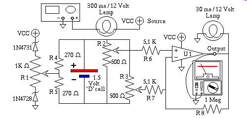
If the meter reads low, rotate R2 from its center point to something more positive. If you had the presents of mind to consider the direction the pot rotates to be important, and if you are like most people you wired the clockwise end of the pot to the positive terminal of the "D" Flashlight Cell since for some reason when most people see this circuit, with positive illustrated on the top, and the association of clockwise with increasing magnitude, that is the way that most people wire up such a beast. For the benefit of those of you that have no such innate tendencies, I will simply tell you to rotate R2 in the direction that makes the plus input of your Op-Amp more positive than it was. You shouldn't have to rotate any more than about 10% of the full lock to lock rotation the potentiometer permits, before the meter responds by deflecting the needle most of the way to the power supply voltage, in this case 12 volts. If on the other hand the circuit started up with the meter reading a high voltage, I would ask you to rotate the R2 pot the other way to find the point where the meter needle swings down to a low voltage. Next I want you to try to make the meter needle point to a place about half way in between the low, and high readings it attained when it seemed to reach its limits of voltage, both high, and low. This is the "Q-Point" for this circuit.
Make a note of what direction rotating R2 correlated with the movement of the meter needle, and now go wiggle the knob of the R3 pot, when you do you will notice that the polarity of the Minus input of the Op-Amp results in behavior of the opposite direction.
Condition 1:
Placing a more Positive voltage on the Plus input of the Op-Amp results in a Positive going output.
Condition 2:
Placing a more Positive voltage on the Minus input of the Op-Amp results in a Negative going output.
Condition 3:
Placing a more Negative voltage on the Plus input of the Op-Amp results in a Negative going output.
Condition 4:
Placing a more Negative voltage on the Minus input of the Op-Amp results in a Positive going output.
The Plus input is given the name Non-Inverting input, exemplified by conditions 1, and 3, and the Minus input is given the name Inverting input, exemplified by conditions 2, and 4.
Adjusting R1 has very little affect, which should come as a surprise to you. Most people upon seeing this for the first time tend to expect the large variation that R1 can deliver to have a major effect on the circuit, but it doesn't, this is because this amplifier is sensitive only to the Differential voltage of the two input transistors, not their individual voltage to ground. This parameter of Op-Amps is called Common Mode Rejection, and it is in part why Op-Amps are so useful.
I built the circuit on a Global Specialties Solderless Breadboard and I can tell you it works fine on both 12 volts, and 17 volts, note: two nine volt batteries wired in series yields 18 volts, which is close enough I will risk stating that your circuit should work with two nine volt transistor radio batteries wired in series to provide the main Positive VCC supply.
The thumbnail shown below is primarily for X, Y, coordinate reference. The real pic, is this Hi-Reso version of it. The idea here is, you're suppose to open up another desk-top in your X-Windowing System, and point the browser to the above link, allowing the Hi-Res pic, to fill the whole screen. Now you can switch from one desk-top to another, instantly, to allow you to get the magnified view to examine some detail, and then back again to read, the location list below, to examine a new part. The Eks, and Wie coordinate pairs are formed by extending an imaginary line from the letter or number nearest that edge of the Solderless Breadboard, and then by following the column, or row of holes, using the holes as gridlines, that way I get the gridlines for free, and I can present you with a picture that is free of the proverbial "Circles, and Arrows, and a paragraph on the back of each one" with apologies to Arlo Guthrie.
 Coordinate   External Bias Circuit
 Eks    Wie   Reference Designators
 C.8 -  7.7 = --      1N4731
 E.0 -  3.9 = R1      1.0 K ohm pot
 D.0 - 15.0 = --      1N4728
 I.5 -  5.2 = R4      270 ohm
 F.9 -  2.3 = R5      270 ohm
 A.0 -  3.5 = --      1.5 V "D"Cell
 H.0 -  3.9 = R2      500 ohm pot
 K.0 -  3.9 = R3      500 ohm pot
 C.0 - 11.2 = R6      5.1 K ohm
 F.1 - 11.0 = R7      5.1 K ohm
 D.5 - 13.7 = R8      1.0 meg ohm
 S.7 -  2.5 = 300 ma / 12 Volt Lamp
 M.0 - 13.0 = 30 ma / 12 Volt Lamp

 Coordinate   Inside of U1
 Eks    Wie   Reference Designators
 E.2 -  6.6 = D1      1N4148
 E.0 -  8.5 = D2      1N4148
 F.2 - 11.2 = R1      3.3 K ohm
 F.0 - 14.3 = D4      1N4148
 F.6 - 16.0 = D5      1N4148
 E.9 - 12.5 = R2      5.1 K ohm
 F.3 - 13.0 = R3      5.1 K ohm
 F.6 - 13.8 = Q3      2N3904
 G.9 - 14.0 = Q4      2N3904
 F.7 - 15.2 = Q5      2N3904
 G.5 - 16.3 = R6      5.1 K ohm
 F.3 -  9.6 = Q1      2N3906
 G.7 -  9.6 = Q2      2N3906
 F.5 -  8.0 = R4      10 K ohm
 H.4 -  8.0 = R5      10 K ohm
 H.6 - 12.3 = Q6      VP01
 I.7 -  9.9 = Q7      VP01
 I.3 -  8.1 = R7      470 ohm
 L.1 -  6.9 = Q10     2N3904
 L.2 -  9.0 = R12     22 ohm
 K.5 - 13.7 = Q8      2N3904
 K.6 - 12.3 = R8      5.1 K ohm
 J.9 - 14.1 = R9      5.1 K ohm
 J.2 - 15.5 = Q9      2N3904
 I.7 - 13.8 = R10     5.1 K ohm
 I.1 - 15.8 = R11     5.1 K ohm
 L.0 - 14.2 = R13     22 ohm
 K.7 - 15.3 = Q11     2N3906
Yes Virginia, the small bulb is lit, and the large one is out. You may have
noticed if you tried to read the values of resistors and the like that I
have taken certain liberties in building this circuit. One thing in
particular, that ought to be obvious, is the "D" Cell has been
replaced with a "C" Cell battery holder, and since I didn't have
any "C" cells on hand I pressed a "AA" Cell into service.
The "P" channel MOSFETs are VP0106N2, again no big deal. In fact
I have made many such substitutions, partially in an effort to make sure
these kind of garden variety parts will in fact work.Xoscope / Siggen:
The following instructions apply if you are using your sound card as a test instrument. I provide links to Linux/Unix programs Xoscope and Siggen, but the information I give here is general enough that you should be able to use it with any operating system, if you obtain the necessary software. Writing your own software to drive the soundcard directly is not all that difficult for one who is familiar with assembly language programming, and interrupt driven, DMA programming, essentially any rocket scientist between 47, and 50 years of age should be able to do it :-) or, perhaps you could just go out and buy a commercial package, but then you would miss the opportunity to learn to write neat low level software. May I suggest that if you feel you have more money, than time, you consider buying a real oscilloscope, and signal generator.
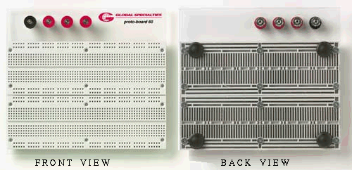
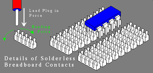
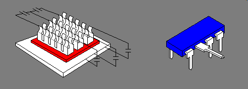
The Global Specialties Solderless Breadboard is an indispensable tool of electronic engineering. To navigate life without one of these little gems is unthinkable by anyone who has used one. Given reasonable care they will last a life time. The second half of this tirade concerns itself mostly with how not to damage this wonderful tool, and how to get the most out of it. Some of what I have to say in that regard has a lot to do with the effects of stray capacitance, and miniscule amounts of stray inductance in the wiring you do on one of these prototyping boards. There are also many vendors of printed circuit boards that will sell you inexpensive copies of the layout of these prototyping boards etched into circuit foils, and pre-drilled with the same hole pattern of the Global Specialties boards so that once you have a working temporary circuit, you can make a permanent printed circuit version of it. Some vendors even supply fairly handsome project cabinet boxes designed to accommodate the printed circuit version of these prototyping boards. I show below a relatively new entry in the Global Specialties product line up. It is a more or less normal pair of Global Specialties plug boards mounted in such a way that they are butted up against one another, but instead of being mounted to metal, they are mounted to clear Plexiglas. This reduces ground plane stray capacitance a little, which may be desirable, but the most important facet of using Plexiglas, is that it is transparent. You can see right through it! I show below the top, or front view, the business end of the proto board, where you stick components into, on the left below, and then the bottom, or back view, on the right. Being able to see into the bottom, one can better understand how these devices are wired up internally. I now will give a little description of what you are looking at. The four round things in the top, are thumb screw / banana jacks, and if you look the right rendition of this device, they are on the mirror image side, since you are seeing the bottom of the device on the right side, this should be expected. For those of you who have never seen these banana jack terminals, they are fastened to the panel by a machine screw nut, usually an 8-32 size - thread pitch. If you look closely you can see the faint outline of the hexagon shaped nuts at the top of the right hand "Back View" shown below. Also on the right the four round things that are twice as large are rubber bumper feet to help protect your table top from scratch damage. The twelve screws appear larger when looking at the bottom, because this is the side of the device that has the heads of the screws exposed. Now I call your attention to the vertical dark pairs of stripes seen in the "Back View". These are the bottoms, of the conductive metal clips that grab hold of, and supply an electrical connection to, components you plug into the prototyping board. To provide you a clearer picture of how these things work, In the next picture I have gened up a pictorial drawing, shown right side up, of the clips themselves, without the opaque white plastic supporting shell framework that holds them in place. In the lower drawing I show on the right hand side a drawing of these paired groupings arranged as metal electrical contact arrays, enough in that sketch to plug an 18 pin DIP, Dual Inline Package integrated circuit into the middle of the array, and for further clarity the illustration also shows an eight pin IC hovering over the spot where one would presumably insert it.
Over size lead wires:
If you ever once, force the insertion of an oversize lead wire into into one of the holes, it will bend the electrical contact beyond the point that it will fully return to its original position. After that has occurred the electrical contact grips normal diameter lead wires less tightly, translation: After such an unhappy event, normal size leads inserted into that hole, are erratic, and noticeably resistive. While it is possible to retention the springy contacts, it's not all that easy for an inexperienced user of hand tools to accomplish. Basically the procedure is, you tear off the backing tape, it's a rather ordinary type of adhesive tape, and set it aside, you may even be able to reuse it. Then remove the deformed clip, then proceed to get out the fine needle nose pliers, and attempt to affect repair. If you've never done this you will probably mutilate the poor little metal clip beyond recognition. I suggest you prove your prowess in this area to your self by making one out of a tin can lid first, then when you feel you are good enough to do it for real, go for it.
Soldering:
Don't solder a wire while it is plugged into the solderless breadboard. Two very bad things happen, one, the heat melts the plastic hole guide, no fixing that, and second most component leads are tinned to facilitate good soldering. Unfortunately this tin coating can permanently fuse the component to the metal clip, solidly enough that forcing the removal of the component lead will further damage the springy clip. Even worse solder, is often accompanied by flux, and the flux will flow right down the component lead into the spring clip assembly, and coat the nearby contacts with flux. Flux, the proper kind you use for electronic gear, is a resin compound, that is a good insulator. So what you've just done is to solder the component lead to the clip, and provided a nice insulative coating on all of the other contact points in that five hole set.
Dirt:
Clean the leads off before you plug them in. You may not realize it, but often the resistors you get to work with came from tape reels that were intended for automatic insertion by a low paid, highly skilled robot, that works faster than fifty human beings could ever work. That tape as it ages leaves deposits on the lead wire, that if you fail to clean them off, will be cleaned off by the metal clip inside the proto board. Guess where that dirt stays after you pull the lead out. If you think rescuing a keyboard that has had soda pop poured on it is difficult, think how hard it would be to clean a proto board after a similar fate.
TO220 Devices:
Inserting devices into a proto board whose leads are not round presents us with an interesting problem. A flat lead, say for example a DIP IC if you look closely at the leads the wide flat lead will spread the contacts farther out if you plug them in the proper way, than if you plugged them in crosswise. By the way plugging an IC in crosswise serves no useful purpose other than providing temporary storage for the IC, because you have just shorted all the leads of each side of the IC together. Although because of the shape of these leads, and the mechanical construction of the proto board as a whole, an IC plugged in the wrong way won't over tension the springy clip, in fact it will barely stress it at all. A TO220 TAB regulator, or transistor, plugged into the proto board, in the orientation that provides something other than a shorted device, will over tension the metal clips. You can avoid this by grabbing each of the metal leads with a pair of needle nose pliers, and twisting them ninety degrees to their manufactured orientation, before plugging them in. This maneuver causes the thin flat portion of the lead to do the spreading of the spring clip's prongs, and that is less likely to stretch the clip beyond reasonable limits. In the same vein, the recommended wire sizes range from 0.015 inches, to 0.032 inches in diameter, or about 26 AWG (American Wire Gauge) approximately 0.015" to as large as 20 AWG or 0.032" in diameter. A 5 watt power resistor, would be a poor choice because a five watt resistor gets mighty hot, but in this discussion I'm trying to explain how to avoid mechanically stressing the metal clips. The leads of this five watt resistor are 19 AWG or 0.0359" too large, however you can squish the round wire, in the jaws of a pair of long nose pliers, near the pivot point, a little bit, just enough to flatten the lead enough so that if you can insert it edgewise into the clip, without severely deforming the metal clip. I won't say just how far you can carry this technique, it depends a lot on how wide the lead gets squished out. This is because the wide end while it won't do damage to the metal clip, it can take considerable force to get it through the plastic hole. Damaging the plastic hole in this way does not degrade the performance of the proto board as a whole, in fact it actually makes it somewhat more useful in that now wider leads will more easily fit through the holes, while still providing protection from the kind of clip spreading geometry that would degrade the clip.
Things to consider:
Large panel:
If you find yourself building up a proto board out of several Global Specialties prototype building blocks, leave lots of extra room around the edges of the proto board cluster in the center. You won't know why, or what you'll need that extra room for until you need it. But trust me you will need it. Power supplies, meters, potentiometers, and the like are all candidates, I even put an old sixties style rotary phone dial as a permanent component of one of mine. It served as a finite pulse source for advancing counters, and shift registers that were being tested. And be extra careful if you drill into the panel, to avoid getting drill shavings into the holes, 28.35 grams of masking tape is worth 16 ounces of cleaning solvent. :-)
The above phrase is more commonly stated "An ounce of prevention is worth a pound of cure.
Type of panel:
A metal panel is conductive, plastic is not. This has serious ramifications for how the Solderless Breadboard will behave electrically at high frequencies, and at lower frequencies in high impedance circuits. Then there is the middle ground, a hybrid between plastic, and metal, composed of both. In the drawing below, left, I show the parasitic capacitors that are formed from this kind of arrangement.
Clip Resistance:
The specifications I have seen on this claim that a new proto board has an initial contact resistance of five milliohms per terminal, however after use they become polished and that resistance falls to four milliohms per terminal. It's sort'a like wine, improving with time.
Interleaving:
If you have ever paid close attention to cable pinouts of high speed parallel data paths, such as the cable standards for computer hard drives, one thing that jumps right out at you, is that they often seemingly waste every other wire on the cable by grounding it at both ends of the cable. The reason this is done is that placing a grounded wire between two signal carrying wires not only reduces the ground impedance a little bit, but it also acts somewhat like a shield wire to prevent cross talk between the two active signals. If you find yourself having trouble with cross talk on a Solderless Breadboard you may be able to minimize this effect by grounding an unused clip pentet that is between the two signals, even if it means rewiring your circuit a little to place a free clip assembly between the two active signals for the express purpose of using it as a crosstalk shield. The wire carrying this ground current should be as short, and straight as possible, and probably connected to the IC ground or perhaps power pin of a well bypassed IC that whose input you are trying to eliminate crosstalk from entering. I have just slipped in a new term. The term bypass used here is sometimes called AC decoupling it means you place a small value capacitor, such as 0.1 uf across the power terminals to prevent localized voltage sag due to high frequency switching transients, caused by the internal circuitry of the IC itself. Doing this makes the AC thevenin impedance negligibly low, and thus from an AC point of view the power, and ground terminals are indistinguishable.
High Voltage:
I have looked all over, and no one who makes, or sells Solderless Breadboards seems to be willing to state the maximum voltage or current any single clip can withstand, with respect to it's surrounding conductors. This is a shame, because there are ICs that are designed to operate from half wave rectified 120 volt house current. They don't spec the maximum current any two connectors of a clip can pass either. If I state this kind of information here, I would be sailing the uncharted sea of specifying a manufacturers product, without their blessing or approval. But as engineers we need this kind of information, what to do... Well look, physics hasn't changed, and dog gonit you can use the basic concepts of physics to make this kind of determination on your own. For one thing the plastic between the clips is as best as my crude calipers will measure it is .020 inches thick. I'm no expert on plastics, but I can make a conservative guess. My choice was to obtain data on a type of plastic that is usable for electrical contact barriers, but not considered "exceptional" just "good" as a simple data point, just to give us some idea of what range of voltage we can expect to place across, any two adjacent clips.
Polysulfone is a thermoplastic polycondensate is used in electric connectors. This expensive material is electroplatable, and has high strength, good toughness, good dielectric strength, and dimensional stability. The trade name of this particular thermoplastic is Ultrason, I show below some variations on its formulation, versus its dielectric strength.
Polysulfone, injection molding, platable grade.
   Dielectric Strength 380 V/mil

Poly(ethersulfone), unfilled
   Dielectric Strength 400 V/mil

Poly(ethersulfone), 10% glass fiber reinforced.
   Dielectric Strength 440 V/mil

Poly(ethersulfone), 20% glass fiber reinforced
   Dielectric Strength 375 to 500 V/mil
As you can see from the above info. the lowest dielectric strength material
used commonly as an insulating thermoplastic is well over 300 volts per
thousandth of an inch, and the wall that I measured was twenty thousandths
of an inch thick. By really simple math the wall between clips should
withstand 6000 volts. However that is not the whole story, the
adhesive tape that holds the metal clips in place could provide a path for
high voltage, and the air where the holes are could also provide an
electrical path. That said, the pins on an IC also suffer from that
weakness, to an even greater degree. Look closely at the normal pins of
the IC depicted in the above right hand figure, notice that the gap
between the metal nearest the body of the IC is considerably
narrower than the spacing at the ends of the pins. If a spark were to jump
the gap that is where it would do it, not down at the insulated holes of the
Solderless Breadboard. If the IC you are testing is designed to
isolate 5000 volts, and they do make Opto-Isolator DIP packages
that do isolate that high of a voltage, across the rows of pins, not adjacent
pins, if the dielectric strength of your ground plane insulator the red
portion in the figure above left is at least 5000 volts then
from one row of adjacent clips to the other row of adjacent clips the
Solderless Breadboard as a whole should withstand that much voltage for
a short period, in dry conditions. As for adjacent clip breakdown voltage
if you stick a mechanic's Feeler Gauge between the gap in
the metal right next to the body of an IC you read about fifty
thousandths of an inch. Using the ten thousand volts per inch rule of thumb
for the breakdown of air, we get 500 volts as an absolute
maximum breakdown voltage of adjacent IC pins and since these
Solderless Breadboards are designed for use with ICs it is logical
to assume that although the insulation from clip to adjacent clip, is
much better than that, the engineers who designed Solderless Breadboards
certainly had no intention, or requirement to design beyond 500 volts of
breakdown protection.High Current:
So what about maximum current they don't spec that either. Well maybe not but they did tell us how much resistance the contacts are. Heres an experiment, put some low voltage, not more than 10 volts, across a low value 1/4 watt resistor, such that it will dissipate the full one quarter watt. You get to pick the resistor based on your stock, using ohms law, and the power relationships I talked about in lesson 009 where I first introduced you to the twelve equation "pie" chart. Dial in a voltage that will heat the resistor with one quarter of a watt of power. Allow a minute for it to heat up, then touch it to feel its temperature, noticeably warm, ok now dial down the power to one tenth of a watt, hmm, that's better. If an object the size of a quarter watt resistor can free air dissipate a tenth of a watt, well enough that you can touch it without any sensation of heat, a metal clip almost twice that size will likely not fare any worse. So I will take it as read that we agree that it is permissible to pump one tenth of a watt into the clip. Ok now if the clip is 0.005 ohm the current we may safely apply to the clip is the Square root of Power divided by Resistance.
            _________
           /  0.100
3.162 =   /   -----
        \/    0.010
So the current we may safely put through a clip is a little more
than 3 amperes. If you noticed I accounted for the fact that it
takes two contacts to complete the circuit through one of these clips.
That's why even though they spec 5 milliohm, per contact my
calculations used 10 milliohms.The purpose of this exercise is to demonstrate that in the absents of complete information about a component you can derive useful and meaningful specifications for the devices you use.
Philosophy of approximation:
In truth I've probably oversimplified the approximation of both adjacent terminal breakdown, and metal clip current. One thing to be aware of concerning current is that all of the one tenth of a watt is dissipated on a tiny region where the metal clip makes point contact to the lead wire. If heat is generated faster than it can be carried away from the point contact and spread throughout the metal clip, that point contact is likely to become hot enough to soften, and perhaps oxidize the nickel plated finish. What these "back of the napkin" calculations do is give you a figure, that is, in the American vernacular, "in the Ball Park" meaning it can be used as a guideline, not to be taken as scientifically rigorous information. As engineers we often use these loose guidelines, in the absents of solid information, and fine tune the details experimentally. Most of the time nothing more is required.
The cascode amplifier:
This one is tricky to get usable information out of without decent equipment. It should be possible though, even if you only have a sound card for producing, and measuring signals. If you're using Siggen, and Xoscope, a quadrophonic sound card may allow you to run both programs simultaneously, or if you have figured out a way to get two separate sound cards interfaced on the same system. The idea here is that you want one of the programs running on one audio device file, say for example /dev/dsp0 and the other on a different one, like /dev/dsp1 since they are two separate programs written by two different authors, each program wants to have the entire interface to itself. Linux loves networking, and if you have more than one machine strung together that will be a workable solution as well, eg. one machine serves as Signal Generator while the other serves as Oscilloscope. In the absents of those alternatives I suppose one could record the signal onto a cassette, then shutdown the Signal Generator, rewind the cassette, start up the Xoscope program, and use the cassette player as a "cough" signal generator. :-)
In the schematic below I have designed two intentionally similar circuits for side by side comparative analysis. The one on the left is a simple common source amplifier, while the one on the right is an almost identical amplifier with one major twist. It is a Cascode Amplifier. The Cascode configuration is a special way to combine both Common Emitter, and Common Base amplifiers into a single stage, to harvest the best attributes of both... Kind'a...
The Common Emitter amp is in this version of it, replaced with a MOSFET wired up as a Common Source amplifier in both the left and right halves of the schematic. The thing that's different about the right hand circuit is that the drain is connected to an emitter of a 2N3904 transistor, whose base connection is hard wired to what amounts to a 5.1 volt powersupply. This pretty much insures that the emitter base junction of the 2N3904 transistor 0.7 volt will hold the emitter at 4.4 volts. However the current that enters the emitter will mostly go via the collector of the 2N3904, and therefore the output of the circuit appears at the collector of the 2N3904 transistor, if a suitable pullup resistor can keep the 2N3904 out of saturation. This does seem like a really round about way to build an amplifier, considering the one on the left is a whole lot simpler.
Stray Capacitance:
Every amplifier of the general type Common Emitter and these include Common Source FET/MOSFET, and Common Cathode Vacuum Tube amps as well, are, plagued with three capacitors inherent in the amplifying device itself. At high frequency these tiny amounts of capacitance are a serious problem. Even at low frequency if the impedance is high enough they also play a serious role. In this particular circuit two of these parasitic capacitors are made to be serious at low audio frequencies, in the range of 1000 Hz and therefore this experiment is devised as a means for you to gain first hand experience with these effects using low cost equipment.
There are three, one between the Source and Drain, one between the Source and Gate, and one between the Drain and Gate. Tubes, and Transistors also have the same stray capacitance on their respective counterpart lead wires. If we could eliminate, by process of magic, these capacitances within the device crystal itself, the lead wires would themselves become our enemy. However capacitance is only a problem if voltage changes. If we can design a circuit that did not have a voltage output, then the parasitic capacitors would become irrelevant. This is one of the goals of Cascode design. The Drain to Gate capacitor is small, compared to the others, by about one third, however the gain of the amplifier makes this a much bigger problem than it might be. The voltage gain, in this case is nearly 200 and it as I have mentioned before is inverted, which means at high frequencies the voltage gain of the amp works through the parasitic capacitor to cancel the incoming input signal! In this circuit I have optimized this effect by making the input impedance ten megohms, and I provide what are effectively two amps, one an ordinary common source, and one that has a cascode stage to prevent any voltage output at the Drain of the MOSFET on the right. Instead the currents are translated into voltage at the collector of the 2N3904 transistor, and thus there is no path for changing voltage to effect the Gate of the right hand MOSFET.
This technique solves the Source to Drain capacitance, and the Gate to Drain capacitance though not eliminated is now only a capacitance, not an amplified counteracting capacitance, that fights the input. The other parasitic capacitance that is not really dealt with is the Gate to Source capacitance, but the thevenin of these is simply two capacitors in parallel and therefore much more easily compensated for with an inductor.
They have a name for this amplified counteracting capacitance, that fights the input. They call this phenomenon, the type of behavior exhibited in the left hand Common Source amplifier, the Miller Effect, and one can choose to view it as a kind of thevenin equivalent capacitance, the formula for which is:
C-equiv  =  RTC * (1 + Av)

Where:

C-equiv  =  The equivalent
            "Miller" capacitance

RTC      =  Reverse Transfer
            Capacitance

Av       =  Voltage Gain (Voltage
            Amplification factor)
The Miller Effect is if you look closely simply stating the
obvious. Many courses dwell on such things, giving them undue emphasis,
I would rather say knowledge of the Miller Effect is mostly
useful for communication with your peers, that were trained to think that
it is a big deal. What is important here is that you truly do understand
why capacitance even though small across inverted output and the non
inverted input is such a big deal. Partly because it is gain
dependent and because gain is somewhat unpredictable, especially when
Miller Capacitance is in play, rather than live with it, and
trying to compensate for it with additional capacitors, coils, and or
feedback, you are better off using a scheme such as the Cascode
configuration shown above right, the rest of the capacitances you have
to deal with are much more predictable, and therefore more easily
compensated.The other great benefit of this circuit is that that usually the high gain device, is generally not well suited as a high voltage device. In VGA color monitors there is a circuit board plugged into the end of the neck of the Cathode Ray Tube. That board is what amplifies the color information to usable levels. An LM1203 color processing chip has analog outputs for Red, Blue, and Green, which are video information. Video is in the range of 70 Mhz and the voltage swings to go from black on any color, typically 150 Volts DC to white typically 40 Volts DC is a signal voltage of 110 Volts peak to peak, in other words it is both high voltage, and high frequency. The three Video amplifiers that drive the cathodes of the three color electron guns, are Cascode Amplifiers.
The Experiment:
Wire up the above experiment, and inject a low frequency like 50 or 100 Hz and you should observe both amplifiers behaving the same, but as you increase input frequency, the common source amp will roll off more quickly than its cascode counterpart. Try swapping the two MOSFETS this should make little difference. In my experiment the common source amp was half the gain of the cascode amp at only 1000 Hz. Also try measuring the AC voltage at the drain of the right hand MOSFET, it will be zero, even though the output is a direct result of that MOSFET's output, taken from that very same drain lead