If you are a student of my webpage I welcome you, but please keep this notice in mind, and plan on re-reading this unit when this notice goes away, as that is your signal that I consider it to be in finished form.
Up to now diodes were thought of as their first approximation, for the most part. The first approximation of a diode, is the notion that it is a one way conductor of electricity, if you attempt to apply a positive potential to the anode of a diode, with its cathode less positive, or negative respectively speaking, the diode rewards you by conducting electricity. The reverse of this is not the case. Application of negative voltage to the anode with respect to the cathode, in this, the simplest view of a diode, causes the diode to switch off stopping all current from flowing.
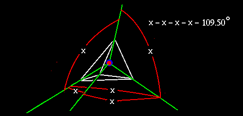
This first approximation of a diode will adequately solve a large body of the day to day work you do with diodes, but they are much more interesting a device than this first approximation lets on. Understanding the diode beyond the first approximation, eases you into solid state physics, enabling you to understand transistors, FETs, thyristors / UJTs / DIACS, avalanche-diodes, constant current diodes, and Zeners / Tranzorbs. If you factor in the external influences of heat, light, magnetic / electrostatic fields, and the action of certain chemical reactions with the air surrounding a specially treated exposed solid state crystal a myriad of sensors become possible. Materials we traditionally use for solid state semiconductor manufacture have a Proton count, and therefore a corresponding electron count, that leaves the outer valence shell, the so called octet exactly half filled, eg. four electrons are in the outer shell. With four electrons in the outer shell, for the Proton, and Electron charges to remain in balance, and the valence charge to still add up to eight, the material forms groupings of atoms that share some of the other electrons to achieve this. Specifically the outer four electrons share one electron from another adjacent atom to balance the electron octet. So what about the other atoms, they share too don't they? Yes, and the result, in the case of a mono crystalline semiconductor is a tetrahedral matrix, that I may someday try to draw as a stereo image, or create an animation where the object rotates for this website, to give you a realistic 3D conception of a tetrahedral matrix, a heroic effort even considering all the molecule rendering packages available under Linux.
For now, I will try to describe what one of these things look like. Can we say that a photo fails miserably to depict such a complex form. Imagine every atom has four points radiating out in all three dimensions, at 109.50' meaning 109 degrees, and 5 minutes of arc from each other, or in lay speak if you were the individual atom centered in an equilateral pyramid, that is a pyramid whose walls are made up of four equilateral triangles, each of the points of the pyramid relative to your position at the center of the pyramid forms a line radiating out from you into space, and there are exactly four such lines.
I touched on what electrical conductivity is back in lesson 006 Measurement in a simple circuit I now will go into a little more detail. Certain types of crystals, molecular, ionic, and covalent, are poor conductors of electricity while metallic crystals are very good conductors. There are some elements, such as germanium, and silicon, what I have referred to as mono crystalline semiconductors that have conductivities between these two extremes. To explain these properties the band theory of solids was developed.
Ignoring for the moment the influence of other nearby atoms, that is their charges, and forces that permit bonding, covalent, ionic, etc.; I will attempt to give you a mental picture of how these electron orbitals are filled.
Every orbital holds up to two electrons. The proton count in the nucleus, determines the number of electrons, each one paired with it's proton counter part. If a lone electron fills an outer orbital, and if there are no more available to fill it, the orbital is said to be half filled. So called electron spin, is negated, or averages out to zero when two such electrons occupy the same orbital. This is not the case when a lone electron is occupying that orbital. An unbalanced spin makes the material magnetic. The term magnetic here means only that the material can by acted on by magnetism, that is it can be weakly attracted by magnetism, and certainly not a magnet itself. This property we call Paramagnetism the lack of paramagnetism, has another name, but if I tell you it's name, diamagnetism I open up an area of much confusion, the very idea of a material that possesses anti magnetic properties, that is a material that is repulsed, albeit very weakly, by a strong magnetic field is the sort of thing that boggles the mind, so I won't even so much as mention diamagnetic materials on my web site. :-)
While we're not on the subject of diamagnetic materials here's a link to a relatively inexpensive diamagnetic levitator project you can build at home in your kitchen to actually see this phenomenon in action.
http://scitoys.com/scitoys/scitoys/magnets/suspension.html
Ferromagnetism is normally what you think of when you think of something that possesses magnetic properties, and it is a special case of paramagnetism. The namesake is from element number 26 it's Iron, or Ferris, as in Ferris-Wheel
The orbitals themselves are really nothing more than fields of three dimensional statistical probability, that map the likelihood that an electron will be found at any given point in this probability density map. In solids individual atoms are so tightly packaged together, that some of the orbitals overlap. If the outermost electron shell, called the valence shell or valence band is either vacant, or partially filled, and is unbroken, eg seamless, throughout the lattice, because of that orbital being overlapped by the same orbital of another adjacent atom, and another, and another, and so on; it is called a conduction band
If an electron is sufficiently excited by an applied voltage, within the crystal lattice, to cause it to jump state to the conduction band it can travel through the lattice without ever belonging to any one atom. This is what we call a free electron. It's rather like floating across a lake, as opposed to crossing the lake by walking via one stepping stone at a time, the predominant form of locomotion in a P doped semiconductor material. A good metallic conductor will ideally possesses a property that the conduction band and its under pinnings the outer valence shell are at nearly the same energy level. making it effortless to promote an electron to the freedom of the conduction band. Of equal importance to metallic electrical conductivity is that these free electrons not be pulled from their free state back into some other atom. In insulators the opposite is true outer valence shell's energy level differs greatly from the conduction band, if it exists at all as an unbroken, contiguous unit, making free electron transfer very difficult. Semiconductors of course fall somewhere in between.
Orbitals have distinct geometric shapes, and this accounts for the shapes of crystals that are formed by various elements and chemical compounds of more than one element. Throughout history to facilitate communication, we humans have given names to things we cannot see, but believe are there nonetheless, based repeatable observations under controlled conditions. Orbitals are given single letter names, prefaced by shell number, and sometimes, where necessary, we assign them an additional designator to indicate which plane orientation they are in, x, y, and z. The shell number, is the same thing as the row number in the periodic table. In truth even the simplest atom possesses the complete set of orbitals, there are probably many many orbitals beyond those known to human kind. I can illustrate this point by a thought experiment. Imagine you are alone in the vacuum of space. Situated directly in front of you, at a distance of a mile or so, is a lone hydrogen proton, that is a hydrogen atom, stripped of its only electron. You are armed with an extra electron, and a Pool Cue. You very carefully shoot that electron toward the hydrogen proton. It is a stunningly lucky shot. The lone proton, happily marries up with the lone electron. But what about the energy states that the electron had to transition to get there. Each transition emitted a photon of light, until the electron was happily seated in the 1s orbital. If there were a single orbital large enough to extend between you and the mother proton, it is possible that a single transition could get the electron there. This single transition, reaching from you, a mile away from the proton, in an orbital of as high an energy, as they ever get, dropping, that is transitioning to the lowest energy a hydrogen atom can possess. Thus, generating a single photon, of the highest energy, the simplest of atoms, hydrogen can have. The photon released is already in the mid ultraviolet frequency range. But that's not the only possibility its trek could have taken, it may very well have stopped at every energy level along the way, releasing a large number of frequencies that extend all the way from radio, to mid ultraviolet light. Or it could have skipped some of the energy states to create still other frequencies in between. Note: All of this ignores the effect of conduction bands, orbitals that overlap to form regions where electrons can move freely between them without actually transitioning from one energy level to another
The order these are in, are as follows:
Note the number of electrons an orbital
can hold is two, one for each spin state

Shell #    Letter name   # of orbitals
   1            s             1
   2            s             1
   2            p             3
   3            s             1
   3            p             3
   4            s             1
   3            d             5
   4            p             3
   5            s             1
   4            d             5
   5            p             3
   6            s             1
   4            f             7
   5            d             5
   6            p             3
   7            s             1
   5            f             7
The above table is not all that important, but it saves me a lot of
explanation. It is arranged in ascending energy, or electron fill
order. Top being the lowest energy, eg, the first electron orbital
to be occupied is the 1s an in the example of hydrogen. Proceeding
down the chart Shell # is a corresponding row number
proceeding from the top of the periodic table downward. Each
Letter name designation has a corresponding number of
orbitals associated with it, the "s" orbitals have one each, the "p"
orbitals have three each, "d" have five, etc.Some examples:
Sodium, also known as Natrium, hence its strange abbreviation in the periodic table "Na" is a conductive metal. Sodium atoms have filled 1s, 2s, and 2p orbitals; therefore the corresponding bands in the solid are also filled. The 3s orbital of sodium, however, is only half filled, eg. one electron, remember it takes two electrons to fill an orbital. This leads to a half filled 3s band. Beyond that point higher energy bands are completely empty.
When a voltage is applied across sodium, electrons in filled bands do not promote electron flow because orbitals in the same band on neighboring atoms are already filled and thus cannot acquire an additional electron. In the 3s band however, which is half filled, an electron may hop from atom to atom in much the same way as one might cross a stream by stepping on exposed stones. Using the "Stepping Stone" analogy this only works so long as there are no missing stones along the path.
We refer to the outer band containing the outer shell, the valence shell as the valence band any band that is either vacant, or partially filled, and is uninterrupted throughout the lattice is called a conduction band In metallic sodium the valence band and the conduction band are one and the same. An important distinction to be pointed out here about the "Stepping Stone" analogy used here with metallic sodium, and one I later use in describing how current travels through a P doped semiconductor, is that these electrons, moving through metallic sodium are doing so, by stepping on stones, or occupying orbitals that are so close together, that they overlap, meaning that the orbital they are in is not owned by a single atom, but more than one, thus providing a path that connects from one atom to another. In metallic sodium it is as if you are crossing a stream that has so many rocks to stand on that the water was merely trickling through the cracks between them, and each step you take is supported by several rocks; meaning the the half filled orbitals are so numerous that any free electron is simultaneously occupying the orbitals of several atoms at once. In a P doped semiconductor the mode of current flow fundamentally different, as will be shown.
In magnesium the 3s valence band is filled, once again electrons in filled bands don't promote electron flow because orbitals in the same band on nearby atoms, being already filled, cannot acquire an additional electron. However, because the crystal lattice is so densely populated with atoms, the vacant 3p conduction band actually overlaps the valence band and can easily be populated by electrons when a voltage is applied. This causes magnesium to also be a conductor. Continuing the analogy this kind of conduction is rather like floating across the stream in a boat, or perhaps walking across the water, something anyone can do if the stream temperature is sufficiently low :-)
In an insulator the energy separation between the filled valence band and the conduction band is very large. This separation prevents electrons from populating the conduction band under an applied voltage. This is like encountering a stream, that is liquid, without exposed rocks to step on, and not a boat in sight.
A semiconductor, such as silicon, and germanium, has a relatively small gap between the valence and conduction bands. Thermal energy promotes some electrons to the conduction band where they are then able to move through the solid. An electron freed in such a way, travels much the same way any electron travels through any conductor, bouncing into an orbital of a nearby atom causing it's charge to temporarily unbalance, and either spit the offending electron out, or accept it as its own, rejecting its own electron, thus freeing it to travel through the, in this case semiconductor.
There is however a whole other important way that charges move in semiconductors. The holes that electrons leave behind cause an imbalance in charge, and the sucking sound you hear, is the electrons of nearby atoms fleeing the safety of their happy home, their mother atom, to move into this new atom's orbital. Their leaving causes a lot of grieving, and ultimately results in an imbalance of charge on the part of the broken home they just left. The mother atom now possesses a net positive charge, insuring it won't be long before a stray electron finds it irresistible. Many electrons will change the atom they call home but sooner or later all of them will be docked, and the conductive nature of their activity is at that point ended, resulting in the semiconductor reverting back to being a perfect insulator. That is assuming that heat, remember room temperature is mighty hot, when compared with the cold of Absolute Zero, isn't busily breaking free more electron/hole pairs to continue moving about the place, what an incredible chaotic mess. Ok for just a moment let's assume we place the intrinsic semiconductor in an Absolute Zero Ice box, let it chill out for a while, but current still flows, well so much for science, I never did believe that stuff anyway... Not!
What is going on here is the fact that the edges of the semiconductor crystal have no atoms to share with, so they have a net charge, or another way to look at it, is to think of them as permanent holes, that can carry charge. I show below a crude partial rendition of the periodic table, in which I have highlighted the elements that have the potential to have semiconductive properties, by virtue of the fact that they have exactly four electrons in their outer shells, and can link up together into a tetrahedral lattice, with perfectly balanced charges.
----                                               ----
|1 |                                               |2 |
|H |                                               |He|
-------                             -------------------
|3 |4 |                             |5 |6 |7 |8 |9 |10|
|Li|Be|                             |B |C |N |O |F |Ne|
-------                             -------------------
|11|12|                             |13|14|15|16|17|18|
|Na|Mg|                             |Al|Si|P |S |Cl|Ar|
-------------------------------------------------------
|19|20|21|22|23|24|25|26|27|28|29|30|31|32|33|34|35|36|
|K |Ca|Sc|Ti|V |Cr|Mn|Fe|Co|Ni|Cu|Zn|Ga|Ge|As|Se|Br|Kr|
-------------------------------------------------------
|37|38|39|40|41|42|43|44|45|46|47|48|49|50|51|52|53|54|
|Rb|Sr|Y |Zr|Nb|Mo|Tc|Ru|Rh|Pd|Ag|Cd|In|Sn|Sb|Te|I |Xe|
-------------------------------------------------------
|55|56|57|72|73|74|75|76|77|78|79|80|81|82|83|84|85|86|
|Cs|Ba|La|Hf|Ta|W |Re|Os|Ir|Pt|Au|Hg|Ti|Pb|Bi|Po|At|Rn|
-------------------------------------------------------
Elements to the left of those highlighted have three electrons in their outer shells, and elements to the right of them have five electrons in their outer shells. Barring other factors the elements on either side of the semiconducting elements are useful for doping the semiconductor. Other factors, that rule elements out as far as their suitability as semiconductors, or doping agents, are things like the relative size of atoms you might want to use as a doping agent if grown into the crystal lattice, need to be as near as possible to the size of the semiconductor's atom, if not, stresses on the crystal lattice as a whole make its behavior less predictable. As a side note there is a technique called interstitial doping, in which a tiny, by comparison to the semiconductor element, dopant is injected into the semiconductor material, this technique is primarily used in Integrated Circuit manufacture, although to be fair most modern devices benefit from many of the techniques learned in Integrated Circuit design. As for choosing an element to use as the semiconductor itself, you are wanting to find a material that has an unbroken conduction band isolated just enough from a filled valence band that while not quite an insulator, it is not a metallic conductor either. This pretty much rules out element 50 Stannous or Tin by name is a conductive metal, hence not a good candidate for a semiconductor. Element 6 Carbon by name has always fascinated me, as an as yet unexplored material with possible uses in semiconductor design. It has a tetrahedral crystalline form, we call diamond, and if one could be grown in the lab, and doped appropriately we just might produce a transistor with unheard of thermal stability, and power handling characteristics, not to mention because of its transparent nature if it were grown as a laser diode the combined power handling capacity of diamond, and the high efficiency of a visible light transparent lasing medium might make an awesome hand held James Bond laser. This is ofcourse pure blue sky speculation on my part, I haven't run the numbers, or even kept up with available research in this area.
Doping:
A long piece of intrinsic silicon, or germanium, with electrodes on both ends, normally makes a nice high resistance, resistor, if not a virtual insulator. For this example I will start out with Silicon, element number 14 in the periodic table, as the perfectly purified semiconductor, and yes it does make a tetrahedral crystal that is nearly an electrical insulator. However sprinkling in a tiny bit of a doping element, say Phosphorus, element number 15 in the periodic table, about one atom Phosphorus in 10 to the 8th Silicon makes this virtual insulator a pretty good conductor. Why? Phosphorus has five electrons in its outer shell, four are all that is used to fit into the silicon lattice network, the crystal. So the fifth one although owned by the Phosphorus atom, due to the tight covalent bonding of the other four makes this lone electron super easy to dislodge from is atom. This additional lone electron has nowhere to reside, except the next higher valence band and that, is in reality the conduction band of the mostly Silicon lattice this lone Phosphorus atom is placed into. Because it's an extra electron, we say this type of material is electronegative, hence "N" type material, and as such its surplus electrons behave very similarly to free electrons in a metallic conductor.
Now the case for "P" type material. As before we begin with a long piece of intrinsic silicon, or germanium, with electrodes on both ends, and sprinkle in a tiny bit of a doping element, while the semi, either silicon, or germanium is still molten, say one part Aluminum in 10 to the 8th atoms of Silicon, or if you prefer Germanium as a semiconductor, look left of it in the periodic table, and you find Gallium, element 31, which makes a suitable "P" type doping element for Germanium, at generally the same one in 10 to the 8th ratio. Either case causes the semiconductor a virtual insulator to become a pretty good conductor. Why? Aluminum, as is also true of gallium, has three electrons in its outer shell, four are needed to fill the semiconductor lattice network, and balance the valence charge, but here we fall one electron short of the required four creating an electron hungry atom every so often throughout the crystal lattice. This situation results in a strong willingness to capture any stray electron floating around nearby to balance the valence of the crystal lattice, but as this happens the charge on the atom that lost its electron becomes unbalanced, and either that electron, or one given up by a nearby atom migrates through the lattice going from hole to hole, never finding a permanent home, under the influence of the slightest provocation, eg. external charge; meaning voltage applied across the entire semiconductor crystal lattice. Because the charge moves as a result of an absents of electrons, this is said to be "P" type material. This kind of electric current, is a much different phenomenon from the kind of current that flows in a metallic wire, via free electrons, eg. the conduction band; conversely this current is occurring by the apparent motion of holes, or electron vacancies that appear to move from one atom to the next, in much the same way as marble vacancies appear to move in a game of Chinese checkers. The important difference in this new kind of conductivity, is that rather than the electron carrying charge as a free electron, it is carrying charge through the semiconductor, as a captive electron, that is, anchored to an atom that is physically, immovably held in a crystal lattice. This electron's only mobility method is to migrate by filling valence holes in order to move from atom to atom, a very different mode of charge transportation.
Some perspective:
Intrinsic silicon has a density of 5x10^22 atoms per cubic centimeter. A doping level of about 5x10^14 atoms per cubic centimeter would result in a resistivity of about 10 ohm-cm. This would be a doping level of one dopant atom per 10^8 atoms of silicon or 10 ppb.
    5x10^22
 ------------- = 1x10^8
    5x10^14
As a rough rule, the resistivity changes one order of magnitude as the
doping concentration changes one order of magnitude. Note: an order of
magnitude here means multiply, or divide by a factor of ten. The actual
math to calculate this sort of thing is well beyond the scope of this
laymans / laywomans treatise... I'll go even farther than that,
the actual math of these calculations is far enough beyond the average
physicist who works with this sort of thing on a daily basis, in the field
of IC design that they almost always use charts, graphs, and
nomographs, or they simulate it on a computer, using an IC design
software package. The data that I give you here came from a chart on
page 33 of a book titled VLSI Design by a collaboration of
authors working under the umbrella of AT&T Bell Laboratories.
The name of the specific author for that portion of the book is
C. W. Pearce.Resistivity:
As I glossed over conductivity back in lesson 006 and then again when I covered how resistors are made, materials, carbon in that case, have an inherent conductivity. Whither you call it conductivity, or resistivity, makes little difference as long as you keep the units straight, they are after all inversely scaled with respect to each other. But just like we have standards for linear measure, such as the foot, or the meter, though very different systems of measurement, they accomplish the same end, they were invented to facilitate communicating the length of things in a world wide uniform way. Resistivity is a way of communicating information about how un-conductive a material is.
Units by which resistivity is defined vary and are often tailored for a given type of work. When making wire for instance we in the US speak of resistivity in terms of ohms per circular mill foot this is the ohmic resistance of a material formed into a round imaginary wire one, one-thousandth of an inch in diameter, and one foot long. Another common unit of resistivity is ohm-cm, used widely in physics and chemistry. Its meaning is quite literally the ohmic resistance of a cube of this stuff that measures one centimeter on any given side, with resistance measured from any two opposing faces of the cube. The size of the cube matters. If you had one thousand, one centimeter, cubes of a material that measured 50,000 ohms from any two opposing faces, and you stacked ten such cubes together in series, and measured their resistance across the length of all ten, you would measure 500,000 ohms. Making up ten such arrangements and wiring them in parallel the result when the resistance is measured from any thin edge of the square material to the opposite edge is the original 50,000 ohms. However if you stack ten such squares, on top of each other, the result is once again a cube, but this cube, that measures one decimeter on any given side has a resistance of 5,000 ohms across any two opposing faces.
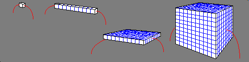
In the above drawing I did not show one important detail. The wires that make contact to the flat faces of the ends of the cubes / rectangle are assumed to be a metal plate of very low resistance that completely covers the entire face, and makes perfect electrical contact with it, eg. no voids or gaps are permitted. And while I'm at it I also need to explain what exactly I mean by ohmic material. Ohmic material is resistive material that is of uniform resistivity throughout the space it occupies in all three dimensions. Ok back to the discussion of the above cube. If you were to obtain a million of these 50,000 ohm one centimeter cubes and wire them up into a one meter cube, it would measure only 500 ohms from any two opposing faces. The reason this is so, has to do with the effective series and parallel resistance geometry of a cube.
Length = Series cubes in the direction of current flow
Width  = parallel rectangles of Length cubes
Height = parallel slabs of Width rectangles

      Length
-----------------  =  ratio of unit resistivity
 Width * Height


        10
-----------------  =  0.1
    10  *  10
I won't go into it here but you can convert any known resistivity of one
geometrical set of units to a resistivity of some other geometrical set
of units. An interesting and useful geometry in integrated circuit design
and hybrid circuit design is to lay down films of a known resistivity,
that are of a fixed thickness. Once this is done, the other two dimensions
determine that actual resistance, and if the shape of the film happens to
be a rectangle, the ratio of length to width, actually determines the
resistance, regardless of the size.The PN junction:
Ok here goes another thought experiment, I give these in an effort to clarify the material being discussed as a series of mental images, not as a practical method of producing, in this case, a real diode.
Magic happens when these two types of material are joined at the atomic level. To accomplish this one raises the temperature of a pure intrinsic semiconducting material to the point where it melts, in an environment that prevents contamination of this precious material. Note Silicon is one of the most abundant materials on earth, think quartz, or sand, Germanium is not far behind, the thing that makes these materials precious, is the enormous cost of refining them to a purity of fewer than one part contaminant in ten raised to the fourteenth power Silicon, or Germanium. This is why IC fabline workers wear monkey suits and look as if they belong in a setting where they are walking on the surface of the moon. The space suits they wear are there to protect the material from the contamination that human beings continually spew into the surrounding air, things like microscopic bits of skin, and material from scent glands are fatal poisons to a semiconductor in a molten state.
At any rate we melt this pure semiconductor, deliberately stir in a tiny amount of impurity that has an outer electron valence electron count one short of the required four electrons, that the semiconductor has in its outer shell. We deliberately pollute the pure semiconductor to one part impurity, say aluminum for instance, in ten raised to the eighth pure silicon. After it is throughly and evenly mixed we reduce the temperature of the mix, to the minimum necessary to keep it in the liquid state. Next we dip a preheated rod into the mix, that has internal plumbing that allows coolant, to circulate near the tip of the rod. We then reduce the temperature of the tip of the rod to a point just below the melting point of the mix and a crystal lattice of "P" type material begins growing onto the end of the rod, and as it does this we carefully pull the rod out of the liquid semiconductor material, at exactly the same rate as the crystal lattice forms. We do this for a while, and as we do we end up forming a long rod of frozen semiconductor material. This crystal rod, has as one of its properties a somewhat better ability to conduct heat, and or cooling. We take advantage of this phase boundary condition, and apply just enough heat to the rod, to arrest the formation of the crystal lattice. Next we cleanse the impurity we introduced, in this case the aluminum we used to pollute the intrinsic semiconductor, by a very simple brute force method, we simply flush in fresh new intrinsically pure silicon, making sure while we do this none of the liquid during the process, forms any new crystalline material onto the end of our rod, and we pollute the new batch with some "N" type material, Phosphorus sounds yummy, each atom has a nice sugary coating of five electrons, we mix it in to the intrinsic semiconductor, but as before, just a pinch, like one part Phosphorus to 10^8 parts semiconductor, and as before we cool it down to a simmer, just enough to keep it liquid. Now we cool down the rod, that is holding the semiconductor crystal rod that has never left contact with the liquid semiconductor, whose material type we have changed during the interim from "P" to "N". This additional cooling of the crystal lattice results in the continued formation of more crystal lattice, but it's now coming from a pool of "N" material, so this portion of the crystal has free electrons that are free to move, as electrons do under the influence of charge throughout the "N" type material portion of this very strange crystal we have just formed.
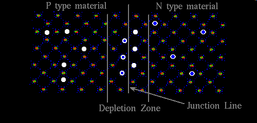
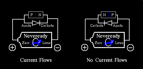
The "N" side of the crystal with electrons to spare, instantly provides negative charges to the neighboring "P" side of the crystal, immediately to the left of the junction depicted above, and although holes cannot really do this, in the sense that the charge migration of "P" material is a phenomenon associated with atoms anchored in place, in the lattice, the hole can move up to the junction, and even across it just enough to steal some of this surplus negative charge that seems to be so abundant to the right of the junction. The result is a depletion zone, where the charges balance, and the depletion zone itself creates an electric field equal to the forward bias potential. This forward bias potential is 0.3 volts for Germanium, and 0.7 volts for Silicon. This can be thought of as a kind of equilibrium, additional free electrons, beyond that required to maintain the electric field, on the right, are repelled by negatively ionized atoms immediately to the left of the junction, conversely positive holes on the left, face a similar fate, as they are attempting to pull a negative charge from somewhere, but every atom immediately to the right of the junction is at present carrying a positive charge. If we apply a negative voltage to the right hand side of the above pictorial, with respect to the left hand side, that is greater than the forward bias potential, free electrons can jump the gap, that is the depletion zone, remember they have to overcome the repulsive force offered by the positively charged holes that have migrated to the right of the junction as part of their, the holes, charge balancing act. But since the "N" type charge carrying electrons are not required to travel by atom sharing in the way that holes are, they can accomplish this, if by no other means than simply occupying holes, effectively crowding them back across the border. Once on the other side, the "P" type side of the crystal, they fill a hole, and then travel from hole to hole, in the fashion which charges normally migrate through "P" material, only to exit out the left hand side on their merry way back to the power source, probably a battery. I've just explained how electric current flows through a diode, given the electrons are flowing into the cathode, and exiting via the anode. Current doesn't flow easily in the other direction. Imagine the same battery now wired up in reverse. The electrons entering through the "P" type material, are carried through to the junction, by passing from hole to hole, one atom at a time, a few of them fill holes at the site of the junction drawing a small amount of current initially, but the act of doing this removes the positive charge that was enticing to the electrons of "N" type region. As this negative charge builds up it begins repelling the very electrons that could have carried current. As this process continues the chasm of charge carrier depleted semiconductor material on both sides of the junction site get ever wider until it stabilizes at some point, the width of the chasm being dependent on voltage. At the moment the system reaches this kind of equilibrium, current ceases, and the diode has cut the flow of current off. So now you see why a diode conducts in only one direction.
Side effects of diode cutoff:
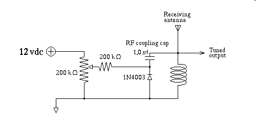
Remember in lesson 011 I mentioned that one of the ways to control capacitance is to adjust the spacing of the plates, widening the chasm, that is the depletion zone, by application of reverse bias to a diode causes it's junction capacitance to change, and it does so in useful, and predictable ways. A common 1N4003 rectifier diode makes a remarkably good Varactor Diode I show a simple variable resonant circuit below, this is the kind of thing that is used in all modern electronic VHF/UHF tuners, like TV tuners, and Police Scanners.
Breakdown:
If you have a pair of terminals spaced a fixed distance apart and you apply enough voltage to them, the air around them will cease to function as an electrical insulator, plasma will form, ionizing the molecules, and atoms that form the air, allowing current to flow, an extreme example of this phenomenon has a common name, we like to call it Lightening, such is the stuff of Zap-Tek Even if you remove the air as a culprit, in a pure vacuum if the voltage is high enough the metal terminals themselves will give up bits of themselves to allow ionization to occur.
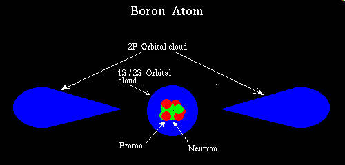
A "PN" junction will also breakdown if the reverse bias voltage is high enough. This point everybody agrees on, but the physics involved is quite a different mechanism than lightening, so far as we know. The older more accepted theory, is one in which the junction diode breakdown is seen as being caused by two different phenomena. The Zener effect, and the avalanche effect. Motorola refers to a kind of Grand unified electric field theory :-) that is called Micro-plasma discharge theory I won't go so far as to call it technobabel, but for a student trying to for the first time to grapple with some of these issues, they will likely christen it, as technobabel. In this discussion I will infuse the basic tenants of both schools of thought, without making the whole utterly incomprehensible. Picture a "PN" junction, in which the "P", and "N" doping are deliberately high, that is lot's of pollution of the otherwise pure semiconductor, with "P" atoms leading up to the junction, and immediately on the other side no "P" atoms at all but lot's of "N" atoms. This would indeed make a diode. Now contrast that with a diode made in which, the degree to which we pollute the semiconductor, is much less aggressive, the goal in the design of this second diode is to sparsely dope the semiconductor. This will also make a diode. Both of these diodes would behave well as devices that conduct well in one direction, and not in the other. They would also both exhibit the property of a forward junction potential commensurate with the given semiconductor material, 0.3 for Germanium, and 0.7 for Silicon. The thing that sets these two diodes apart is their breakdown voltage, and the physics of how the breakdown occurs. Heavily doped "PN" junctions tend to breakdown predominantly by way of the zener effect, and at very low voltage, typically 3.0 volts or less. Lightly doped "PN" junctions tend to breakdown predominantly by way of the avalanche effect, and at considerably higher voltage, typically 7.0 volts or more. A diode doped at a level somewhere in between might break down at 5.0 volts, and be simultaneously both in Zener, and avalanche mode, and the effects of these two modes of breakdown may be contributing equally to the phenomenon of breakdown. The concept of Micro-plasma discharge theory seems to state otherwise, in that it refuses to acknowledge either mode. The main premise of Micro-plasma discharge theory is that once electrons, or rather charges percolate through the "PN" junction in the wrong direction, eg, reverse biased, and at the onset of breakdown, probably at the point of a single cluster of semiconductor atoms, the act of doing this jars loose other electrons creating electron/hole pairs that can provide even more ability to carry charge, and it goes on to state, that this phenomenon rapidly spreads through the entire crystal. The trouble with it is that it fails, as I understand it, to explain the temperature coefficients observed in Zener versus avalanche mode. You see a heavily doped "PN" junction Zeners at such a low voltage, that the depletion zone has not been widened by the reverse voltage. In fact the depletion zone is so narrow, due to the low voltage, and the doping is so great that electron tunneling is possible. Quantum mechanical tunneling is a phenomenon best understood by Extra Terrestrials, and loved by the likes of Rod Serling of Twilight Zone fame. Please bear with me, this gets a little strange. In modern chemistry three dimensional bonding angles are best understood by employing orbital theory. Orbital theory has as its basis many of the tenants of quantum mechanics one of the stranger notions, is a deeper understanding of the true nature of the electron. As we proceed up the periodic table of the chemical elements hydrogen has a single electron, and that electron exists as a cloud of statistical likelihood of relatively even dispersion, spherically about the nucleus of the atom. Mind you this says nothing about the exact whereabouts of the lone electron possessed of a hydrogen atom. With helium, there are two electrons, whose charge is balanced by helium's two protons. These two electrons occupy both the spin states of the 1s orbital. Continuing down the periodic table to the next row on the left hand side is Lithium, element number three, it has 3 protons and therefore to balance the charge 3 electrons. The first two electrons fill both spins of the 1s orbital, and then the last electron half fills the 2s orbital. Next Beryllium, with four electrons, fills both spin states of the 1s, and 2s orbitals. Next we have Boron, with five electrons, it fills both spin states of the 1s, and 2s orbitals, and the last electron drops into the 2p orbital. Both the 1s, and 2s orbitals are of the spherical type seen earlier in the hydrogen atom, although the 2s orbital is considerably larger than the 1s orbital. Boron is the first atom to at least partially fill a non-spherical orbital, namely the 2p orbital. Ok now things get strange, the shape of the 2P orbital is as follows.
In truth I have taken serious artistic license here, that is I have greatly oversimplified the whole subject. Someone once said half the art of teaching is knowing when to lie. The above pictorial is not accurate, there are in fact three sets of P orbitals oriented in the X, Y, and Z planes, and beyond those are the D orbitals which I haven't even touched on, in addition, I neglected to mention the all of these are available to even Hydrogen. Drawing these things in their proper proportion tends to produce a picture that is misleading, because you can't pictorially represent the areas of zero probably and near zero probability in an easily universally understood way, so I exaggerated distances, and stated some things in black, and white, to make a concise point. To come to grips with this sort of thing, is to suspend your sense of reality of the physical world, and replace it with a mathematical model, that does seem to predict all that we observe in the world of the very small. To physicists, and chemists, that have come to use this technique, there is no geometric analogy, the mathematical model is the answer, and it does explain quantum interactions. But the lay people of the world can still tie their shoes, a task impossible for some experts in Superstring theory. :-)
What I am trying to say here is that as a first approximation a physical model of the quantum world will likely serve your needs in electronics, and certainly for day to day calculation, but you should be aware that there are disciplines that do in fact iron out the details, and that while you probably don't want to go there, you should know something about them.
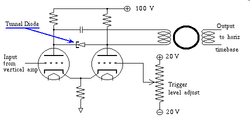
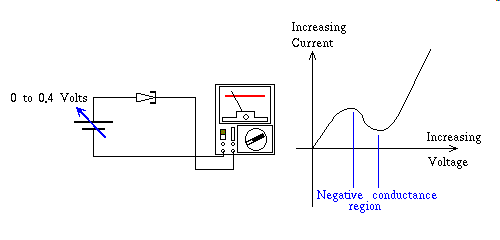
Tunneling occurs when relatively small amounts of electromotive force, over very tiny distances bend the laws of non-quantum physics, just enough to allow electrical current to flow as if some new undiscovered energy state, read that "Orbital" popped into existence for our amusement. Quantum mechanical tunneling only conveys charge across very thin regions of material, eg. on the order of one millionth of an inch, and as I stated earlier only at very low voltage. In the case of Zener diodes, less than 3.0 volts, but zener diodes normally operate in reverse bias all of their life, there is however another semiconductor device that exploits tunneling in the forward bias mode. The Tunnel Diode is a device that starts out as a strong tunnel effect device, as I said in this case, in forward bias mode. It does this at very low voltages, like one tenth of a volt. As you increase the voltage in the forward bias direction toward the normal forward "PN" junction voltage but still far short of that required to overcome the electric field, that is at present repelling free electrons, at the junction site with ionized atoms immediately on the other side of the junction, the voltage, that is the potential difference per atom of semiconductor makes the quantum tunneling effect disappear as this voltage increases. In effect choking off the flow of current seen at the lower voltage. At some point the "PN" junction forward biases now providing current via the normal mechanism, by overwhelming the repulsive force to the electrons, by the negatively ionized atoms just across the junction, and current once again increases. At this point the diode is in normal forward bias mode, and Quantum mechanical tunneling effect has all but disappeared. In summary this feature of quantum mechanical tunneling, diminishing the current, as voltage increases, has been given a name that is the source of much confusion, they call the phenomenon negative conductance. To avoid the confusion, just remember that Tunnel Diodes only exhibit this special phenomenon in the range of zero to three tenths of a volt or thereabouts, and that it is a polarized phenomenon, meaning it does not work in the other polarity, only forward bias, thus you cannot think of this device as the opposite of a resistor. That said the property of Tunnel Diode negative conductance is still very interesting for several reasons. Since it is a Quantum effect, depletion zone charging is not part of the mechanism, and as a result tunneling does not have to wait for charges to build up in a depletion zone for tunneling to occur. So tunneling effects are almost instantaneous. A tunnel diode wired up in almost any kind of a circuit that biases it in the tunnel effect voltage range, finds a way to oscillate, that is, any coil connected to a negative conductance circuit is almost guaranteed to oscillate at the resonant frequency of the coil and it's capacitor. A simple wire is both an inductor and it has at least some stray capacitance to its surroundings, so even a wire is a resonant circuit, and in the presents of a negative conductance even connecting wires oscillate, and they do so at incredibly high frequencies. Oscilloscopes designed to operate in the 100 mhz range need to either compensate for the delay of their triggering electronics, a tedious and unreliable endeavor in the best of circumstances, or find a way of determining the point to trigger the horizontal sweep based on the input voltage, as compared to a reference voltage, using an incredibly fast circuit to convert the differential amplifiers output into a pulse to start the sweep cycle. That circuit is a tunnel diode wired across the diff-amp's output in parallel with a cap coupled itty-bitty toroid transformer to catch the transition, as the current, relatively constant comparatively speaking, but still under the influence of the, now amplified, input trigger signal causes a sudden transition from less than a tenth of a volt, the tunnel mode to several tenths of a volt, the forward bias mode, observed across the terminals of the tunnel diode. The output of the itty-bitty toroid transformer is a pulse that initiates the sweep circuit. These devices in their heyday were very impressive, but here in the technical vastness of the future we now have transistor-like devices inside integrated circuits that can oscillate at 60ghz, that is not an error, this is one sixtieth the frequency of light!
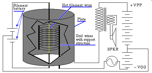
Not to spend time on an old technology you are likely never to encounter, but vacuum tubes are such a simple device, that not knowing the basics of this ancient technology, should we ever bomb ourselves back to the stone age, would leave you quite unprepared to restart civilization. Essentially the act of turning on an incandescent lamp, ya' I know those too are rapidly becoming an ancient technology, anyway, a glowing filament, in a vacuum, with some kind of an electrode, say a cold metal plate, meaning room temperature, inside the same evacuated space where the filament is located will if charged positively with respect to the filament allow current to flow, Thomas Alva Edison, noticed this, and dubbed it the Edison effect. Promptly brushed it aside claiming it to be of no value. DeForest and others investigated further. The mechanism by which electrons flow from a dimly glowing filament to the plate in a vacuum, is because the filament is hot. Heat at the atomic level is random motion, the higher the temperature the more vigorous the motion. This motion tends to shake an electron off, into the surrounding vacuum. An electron has a negative charge, so it tends to be attracted to anything bearing a positive charge. If the plate is positive the electrons go for it, and current flows, if the plate is negative, those same electrons are repelled, and no current flows. Incidentally if on their way to the plate, a widely spaced grid wire is placed in their way, they just merrily go through it, or at least around a given grid wire on their way to the positively charged plate, no problem, it don't even slow'em down. However if we apply a sufficient negative voltage to that same grid, say somewhere around negative twenty volts, those same electrons are now repelled, back toward the filament by the negative charge on the grid, read that Electric Field so they never make it to the plate. Since the grid, is not accepting electrons, even in the discharged state that allowed electrons to pass through the grid, no current flows in the grid what ever. Here's an input that draws no current, read that power, and controls a significant amount of power in what ever the plate is connected to. That is amplification, and amplification is what makes most electronics possible.
Rotary Contact Rectification:
Tubes are ok, but they don't really handle large currents well, 300 milliamperes is about tops for a Vacuum tube, so what if you want more, and you don't yet possess Solid State Diode technology. Well if you can build an induction motor that has small permanent magnets in the rotor, to keep it perfectly synchronized with the AC power source, you can couple the output shaft to a brush assembly wired to switch each half of the sine wave, such that the result is always in one polarity. Ok so it's primitive, but it works very very well. Continuing on with this train of thought, years ago they used to make a device they called a vibrator, it used the principle I outlined in lesson 011 in the Back EMF Experiment, The vibrator circuit is a relaxation oscillator that drives two legs of the primary of a step up transformer alternately to ground, with the primary's center tap connected to the positive 6 or 12 volts, as these were predominantly used in early Automobile Radios to develop the three to four hundred volts needed to get useful power out of the tube circuit. For a while they added an extra set of contacts to rectify the high voltage AC output from the secondary side of the transformer into high voltage DC to meet the plate voltage requirement. This technique more efficiently exploited synchronous electrical contact rectification, as opposed to tubes which lost about 40 to 70 volts in the rectifier tube itself.
Other Esoteric Rectification Schemes:
Flame rectification:
Although I've never seen this myself, I have heard of a scheme to achieve a small amount of rectification at high voltages, eg. thousands of volts. It is used not so much to rectify for the purpose of developing usable DC power, rather the phenomenon is instead used to detect the presents of a flame at the gas jet. You see if the flame goes out, the high voltage corona will only draw current equally, a suitable filter capacitor will only see a net DC charge so without a flame, there's no voltage. With a flame however, a little more current flows one direction, than in the other, providing a net DC charge across the cap, that small voltage is then detected, and used to keep the gas valve turned on. If the flame goes out, voltage goes away, and the control circuit shuts off the current driving the gas valve.
Coper Oxide Rectifiers:
One of the oldest power diodes to grace the planet, and the next to be discussed Selenium, are both part of a class of diodes called Metallic Rectifiers they are in fact Polycrystalline Semiconductors the "PN" junction discussed earlier applies to Monocrystalline Semiconductors. In Metallic Rectifiers electrons flow from the metal to the semiconductor, and not the other way around, in the case of the copper oxide diode the semiconductor, the cuprous oxide, is formed on one side of a copper metal plate, by oxidation at high temperatures. The rated reverse voltage before breakdown is 4 to 8 volts RMS, and they work with reasonable life expectancy up to 60 degrees C
Selenium Rectifiers:
Later another Polycrystalline Semiconductor Selenium was found that operated at considerably higher breakdown voltage. Europe started using them late in the 1920's and the US late in the 1930's and they remained in vogue clear into the 1970's. Essentially these represent a kind of point contact diode, refined to take advantage of modern industrial processes. A simple metal plate, coated on one side with Selenium, the surface area thus greatly magnifying the usable diode area, read that current. A eutectic alloy counterelectrode is then deposited over the Selenium. In the forward biased mode electrons flow from the counterelectrode into the Selenium semiconductor. Reverse breakdown doesn't occur until 20 to 40 volts, and there have even been higher voltage Selenium diodes made, at somewhat higher cost. Their safe operating temperature is, depending on the device, 80 to 100 deg C beyond that they age, much more rapidly, thus severely shortening their life. They were then placed in stacks, effectively wiring many individual diodes in series to get higher reverse voltage. The plates themselves having been drilled so that a bolt sheathed with insulative tubing, and insulated washers at either end, and a nut screwed on the end to apply mechanical force on all of the contact surfaces. By clever arrangement of the order, that is the facing of the plates, and the addition of five power lugs, and a wire to solder the two ends together, a single component full wave bridge was formed. Oh and if you ever overloaded one of these you will remember it for the rest of your life, Selenium is incredibly toxic but once in the air, it oxidizes into a form that is considerably less so. But it smells worse than anything you are likely to be able to imagine. Sorry the HTTP protocol, nor HTML provide the scratch-n-sniff function. Actually I think we are all better off without it.
Thyratron Rectifiers:
Similar to its Ignitron cousin, these are essentially Mercury Vapor Plasma Arc tubes, they can both rectify, and amplify, fairly large currents, at high voltages, and found their way into many industrial process control applications, again these are relics of the past, modern Silicon diodes likely have by now supplanted even the oldest of these, by attrition if nothing else.
Seriously why do I spend time on these:
You need a background in these obsolete technologies because they are relevant in modern design. I will cite one example: Synchronous Rectification has enjoyed a resurgence using modern power Mosfets in place of electrical contacts to achieve unheard of efficiencies, and with greater efficiency, integrated circuits can now create on board high voltage power supplies, making it possible to use a single uniform voltage to power the IC without the IC running needlessly hot. An example of this sort of thing in reverse, and a way to see a little of how Scientists and Engineers think, is to understand that they never make anything more difficult than necessary. SCRs, Silicon Controlled Rectifiers, and TRIACs are in a class of Semiconductor Devices we call Thyristors, in homage to the Thyratron Tube. The physics of a Thyristor isn't anything like a Thyratron Tube so why call them by a similar name? Scientists love simplicity, a Thyratron Tube has a trigger input, that "ignites" the Plasma. Once the Plasma has been ignited, the current is sustained by enormous currents, comparatively speaking, between the main plates in the tube. This continued conduction Plasma does not extinguish until such time as the main power traveling through the tube stops. In other words, you can initiate a pulse to start the Plasma, but you are powerless to stop it after it starts. Such a device wouldn't be of much use if it were not for one small detail. Thyratron Tubes are generally used to directly control AC power. Alternating Current is as I have pointed out many times before a continuously varying sine wave, that spends part of its life at zero volts. This allows the Plasma to extinguish, and since this happens at least every 8.33 milliseconds assuming 60 hz you in fact do have an "Off Switch". As it turns out solidstate Thyristors, behave exactly the same way, albeit using totally different physics. In a Thyristor parasitic positive feedback is what keeps the device "turned on" and the "gate" terminal is analogous to the "igniter". In closing this paragraph everything in science has a connection to everything else, even if we can't figure it out. The passion that scientists and engineers share is one of endless exploration of the physical, endless because no matter how deep you go, you keep creating new doors to open, and as you do you grow spiritually, read that intellectually. To a true scientist, possessed of the passion for learning, stepping off the track to attend the needs of life, is an unwelcome distraction. Almost without exception people in this walk of life know personally a thing some call Flow a euphoric state that occurs when all the material, read that "Acquired knowledge", needed to complete a totally new task, is completely in view, in the minds eye. All that is standing between them and fruition is the act of applying that knowledge. The lure of Flow often overwhelms the baser instincts. Many folks never know Flow I suspect if they did a lot more of them would be programmers and the like. This is a very different thing from a sense of accomplishment, one possessed by Flow has yet to complete the task, nor do they know if it will turn out favorably. The journey is itself the reward, the destination is merely a side effect of traveling the long road. Nothing very useful, or interesting, is to be found at the destination, but the journey... now there's where the gold mine is, meaning learning is taking place. There are more computer programs in the Unix world, on the Internet for free, usually under the GPL, General Public License than anyone can keep up with, you simply can't download them all. I here Window$ users complain that although there are many of them, they are nearly all unfinished works. These people seem to have the idea that a program isn't finished unless it is user friendly, well documented, and is bundled with tech support. That is utterly untrue. Many of them are in the development stage, and the version numbers tell you if that's the case, but the finished ones, that do a single simple job, and do it well, are often left as simple command line driven programs, and are shipped as source code. If you don't like it, add a User Interface to your liking. Where this is going is the guy/gal who wrote the program, did his/her best to get the bugs out of it, they included the source code so that you can make of it what you want it to be, and he/she included the source so that you know everything he/she knows about the program, what better documentation could you ever wish for. But at this point the journey is over for him, or her. All of the exciting stuff has been done, to do any more would provide much less entertainment, and learning. They have likely gone on to start another project that will enrich their lives by teaching them something new. Right now as I make a gigantic leap of faith, I will assume you are visiting this page because you are fascinated with electronics, now imagine a time when you know the subject so well that my page has nothing new to offer. I won't fault you for leaving it, as you pursue other interests in fact I would find it kind'a weird if you did otherwise. That said, don't fault others for doing the same, we all need to grow. So you might ask, why do I write this page. I saw a need, and a chance to learn to write HTML, while integrating some of the wonderful Unix/Linux tools we have available today. The need itself may have been inspiration enough, but the journey... that's the real treasure
In closing this unit:
As for true Monocrystalline Semiconductors we have been talking about intrinsically pure silicon, or germanium, no, or at least very few impurities. The realities of production of early semiconductors, made it awkward to produce doped silicon/germanium followed by the layer free of doping, or even worse a layer of material doped with the opposite polarity doping material, as I understand it, the change over from the region, of "N" type to "P" type material, was often a matter of compromise, as "P" type was to some degree always present throughout the lattice, thus in these early processes, control of the "N" doping was the only economically feasible way to make a transistor or diode, in the one instance I can pin down Phosphorus was used as the "N" dope, since aluminum was always present as an unwanted contaminant, not easily removed, from the otherwise intrinsic Silicon/Germanium. By todays standards these made truly awful devices, leakage currents were high, and unpredictable, as were the gain, and other factors. Thus the simplistic description of deliberately doping with "P", and then with "N" type regions wasn't actually achievable until manufacturing processes became a lot more mature.
As a result, PNP transistors were much more common in those early Germanium transistors, and NPN transistors remained for many years an expensive rarity. By the time Silicon transistors came into widespread use, process control had improved, and Germanium had other weaknesses as well, few people in the electronics world have any idea that modern Germanium devices now sport leakage currents as low as any silicon device. Today it is an accepted, but untrue, urban legend that Germanium is not useful as a semiconductor material for low power electronics, where thermal instabilities are less of a problem. Germanium has other short falls though that do tend to preclude its use, especially in IC design.
Another final point:
In all modern devices doping is actually performed after the pure intrinsic semiconductor crystal is grown, by driving the dopant into the surface of the otherwise pure crystal. Many methods are available to accomplish this, I'll mention one, you bathe the silicon in a gas at elevated temperatures and pressures, and the dopant oozes in. Although it is possible to ooze the dopant back out, it isn't very cost effective. If you dope with a P type material long enough to deeply embed the layer of dopant and then dope with an N type material for a shorter time, the result is a layer near the surface that approximates an undoped semiconductor. Why might this be true? The answer is that with both kinds of dopant present, while the P type is trying to create holes for electrons to fall into, the free electrons provided by the N type material simply fall into the holes, filling them so that they can no longer facilitate charge migration. While this technique is useful, it must be used sparingly, or the entire semiconductor will become less influenced by dopant atoms intentionally added later, and thus will behave less like a semiconductor.