If you are a student of my webpage I welcome you, but please keep this notice in mind, and plan on re-reading this unit when this notice goes away, as that is your signal that I consider it to be in finished form.
Here I try to give meaning to Lesson 016 with respect to Diode approximations What is an approximation? A definition often tells you very little about any significantly involved subject. I can however get the point across by giving you an example of something you know well. The numerical constant Pi is a non-repearing, irrational, number, that on occasion we choose to approximate with a short string of digits like
Pi is approximately equal to 3.1415926
But eight digits, can be too precise for some applications, say for instance you want to compute some rough idea of how many feet of cable are wrapped into a given coil, that you wrapped around your thumb/forefinger, and your elbow. The technique is you measure the mean diameter of the coil, probably with a simple ruler, and count the number of times the cable crosses the same place. Next you multiply that number, times the measured mean diameter, and then times Pi. Since the measurement is of less precision than two significant digits of accuracy, and the count of wraps of cable is an integer that probably fails to take into account the fact that one third of an additional loop of cable was not counted, your result, regardless how precise your representation of Pi is, will be no more than two places of accuracy. If you are doing the calculations in your head, because the calculator is not within easy reach, using an approximation of Pi to only two places of accuracy is more than adequate for this application. To actually grind the number out to eight significant figures is really stupid. If you disagree, I need only to ask you if you are trying to be so precise, if you thought about whither your calculation was considering the length of the plugs on the end of the cable, or not. If you failed to even consider the next level of the approximation of the cables length, the length of the plugs themselves, how can you rightfully be concerned about the precision of your approximation of Pi. Hopefully at this point you begin to see how futile, meaningless, and unnecessary such a high precision approximation of Pi in this example is, and if you were prepared to answer that one, did you do anything to insure that when you measured the mean diameter of the coil, that the cable you were measuring was formed into a perfectly round circle, if the circle isn't perfectly round to start with, high precision Pi won't accurately reflect the length of the cable anyway, whither you are including the plugs on the ends or not. Even more to the point the cable, bundled into a coil in this manner, is lumpy, making it impossible to form a perfectly round circle, that would warrant the use of more than three significant digits of Pi.
If I'm going to measure the height of a building, and I make my measurement before they paint the trim of the top of the building, making it three one thousandths of an inch taller, because of the thickness of the paint after it dries, does this omission void the accuracy of my measurement? What about the temperature of the structural members of the building, failure to take this into account will certainly give an incorrect assessment of the buildings height, unless the building's overall expansion coefficient is zero.
These silly, and extreme examples demonstrate why we have levels, or orders of approximation in engineering. Measuring the height of a dime, before versus after painting might be significant, but the height of a building with or without that extra coat of paint is not significant. A painted dime for instance may not be accepted as the dime it is, in a vending machine, if the dime has been painted, but I think the error in the height of a building resulting from painting will make little difference in whither the building is salable.
If you are building a simple rectifier, with a single peak charging capacitor that is powered from AC line voltage, eg. 120 volts AC, the small forward bias potential of a few tenths of a volt, eg. seven tenths for silicon, will have negligible effect on the voltage the capacitor charges to. On the other hand the same circuit powered by a two volt RMS AC sinewave power source will see a significantly lower voltage than you would normally expect as a direct result of this same seven tenths of a volt lost in forward biasing the diode.
Here's the example of the line voltage
example above.

120 VAC RMS x 1.414 = 169.7 Volts Peak

169.7 Volts Peak - 0.7 Diode drop = 169 VDC

Your error had you not accounted for diode
drop would be...

  169.7
---------  -1  * 100 = 0.414 percent
  169.0


Now for the 2.0 VAC case

2.0 VAC RMS x 1.414 = 2.828 Volts Peak

2.828 Volts Peak - 0.7 Diode drop = 2.128 VDC

Your error had you not accounted for diode
drop would be...

  2.828
---------  -1  * 100 = 32.89 percent
  2.128
As you can see the 120 volt example was not appreciably affected by Diode
Junction Drop, but in a similar circuit powered by only 2.0 volts Diode
Junction Drop is significant.The Junction Drop is not any kind of a battery, well ok if you shine enough light directly onto a diode crystal, it will produce a small amount electricity. What happens is photons fall on the the surface of the diode, and some of them are absorbed, raising electrons out of their normal orbital position. This disturbance reaches the junction, and upsets the equilibrium between the electrons and their holes at the site of the junction. A small electric voltage is formed that is below the Junction Potential, and since it is being continuously replenished by a flood of photons current flows if a path exists across the terminals of the Diode. This is the principle by which solar cells operate. However in absents of something to replenish the charges, such as the aforementioned photons, a Diode's forward junction potential will quickly discharge to zero volts and current will cease.
As the next level approximation when we factor in the Junction Drop we can draw a reasonable approximation by using our earlier model of a diode, and a battery that has the same voltage as our Diode's Junction Potential. This new model, or Next Level Approximation, can be drawn as follows.
       ideal diode    +    -
            \ |        |
------------->|--------| |---------
            / |        |   0.7 volt
You may have noticed I keep using the phrase "sustained current" and wondered why. While the Junction Drop is not a battery a diode charged right up to forward bias potential will deliver a short pulse of current as the charges leak out into a load subsequently connected to this diode. The diode is also a tiny capacitor, and the non-sustained current are those charges leaking off to the load. But after they have done so, all current flow ceases, and for current to be useful, in the sense that it performs work, like the kind of thing a battery does, eg. able to turn the motors of machinery, I can with conviction state, no useful current flows from the junction of a diode, because that current is not sustained.
What it does mean is that in order to forward bias a diode, it takes an additional voltage applied externally of at least the junction drop voltage. Further when the diode is in forward bias mode the current passing through it, multiplied by that junction drop voltage gives a wattage figure that manifests itself as heat.
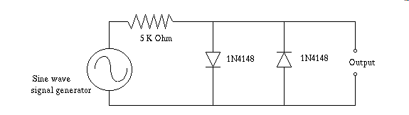
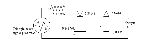
You can take advantage of the phenomenon to do a myriad of practical things. A simple two diode clamp is possible constructed as follows will reliably convert any suitably high enough AC voltage sinewave into something nearly approaching a square wave.
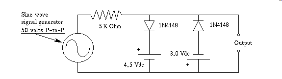
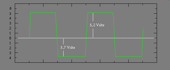
Next I show a more versatile version of the diode clamp, in that it isn't stuck at only producing an output of plus, and minus one junction drop.
Ok these second level approximations are going to give you an appreciation of junction potential, but they are only an approximation that is based on the junction potential being some set value, eg. 0.3 volts for Germanium, or 0.7 volts for Silicon. In the next level of approximation we take a good hard look at this assumption. It's not strictly true. First of all the 0.3 volt, or 0.7 volt, junction potential we have been using changes slightly as a result of the quantity current flowing through the diode changes. The junction voltage follows a negative exponential curve as current through the diode increases, assuming there are no heating effects. Additionally temperature plays a part that causes a relatively linear change in junction voltage as long as we operate the diode near room temperature. Solidstate physics follow mathematical relationships on the absolute temperature scale, I.E. Degrees Kelvin. This scale begins at zero thermal energy. There is nothing colder in the universe than this kind of zero temperature. In fact it is impossible to ever reach absolute zero, because no matter how hard you try some small amount of external heat still will penetrate the walls of your Ice-Box. So we simply take measurements, and work the problem backward, attempting to project the numbers that might occur at absolute zero temperature. Or we use a convenient approximation, based on room temperature. Stated in english it reads for a constant applied current a diode that drops a given forward biased junction voltage will decrease that voltage by 2.5 millivolts for every centigrade degree the temperature is increased. If you wire up a circuit that provides a constant, but low current to a diode, and very carefully measure the junction potential, for moderate temperature extremes this diode can be used as a functional thermometer. Moderate here meaning minus forty degrees to plus 212 Fahrenheit, or 100 Centigrade. What I mean by low current is low enough that self heating, caused by current passing through the diode under test does not appreciably heat the temperature measuring device, namely the diode. In a practical version of this kind of circuit, you would likely use several diodes in series, making the voltage change larger, and therefore more easily detected. Also you might pulse the current "on" just long enough to make your measurement, to keep from heating the diode, and if the device is battery operated this will extend battery life as well.
Notice that I added another caveat, I included the condition that the current flowing through the diode was controlled, that is held constant. Part of the reason this is necessary is that the diode is composed of three regions.
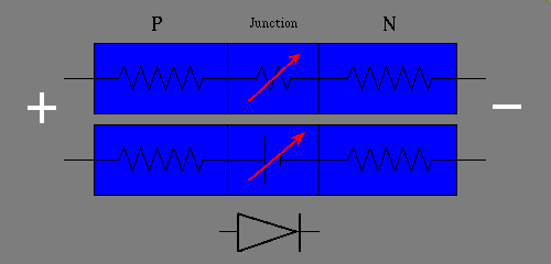
When a positive voltage is applied externally from the "P" side of the diode with the negative side of that same voltage source connected to the "N" side, of the diode, the diode is said to be forward biased. Under forward biased conditions, the external voltage creates an electric field that concentrates across the depletion region. This field is of such a polarity that it diminishes the effect of the inherent field set up by the depletion zone. As a result the net field within the depletion zone is narrowed, and some carriers are no longer prevented from diffusing to opposite sides of the junction. A few electrons spill over from the "N" side to the "P" side and become carriers on the P side. Conversely a few holes spill over from the "P" side to the "N" side of the diode and become carriers on the "N" side. This spill over is called carrier injection.
The carrier injection process causes the current in the forward biased "PN" junction to increase exponentially with the applied voltage according to the following equation:
                      _             _
                     |   vd / n * vT |
id     =   Is   *  ( | e             | -1)
                     |_             _|

Where:

vd  =  voltage applied to the diode

id  =  resulting current that flows through the diode

Is  =  scale current, also called saturation current

e   =  the base of the natural logarithms

vT  =  the thermal voltage

T   =  the temperature in degrees Kelvin

n   =  the emission coefficient
Scale current, AKA Saturation current, AKA Reverse Saturation current, is
a function of the donor and acceptor impurity concentrations in the diode,
as well as the diode temperature, the area of the junction and other fixed
constants. The value of Is typically lies in the
range 10^-8 to 10^-14 amperes for discrete silicon
devices. The value of Is can be as small as 10^-16 amperes
in an integrated circuit diode.The thermal voltage vT is equal to Boltzmann's entropy constant k times the temperature in degrees Kelvin T, divided by the charge q of a single electron in coulombs, sometimes referred to in physics as a constant named Elementary charge.
vT  =  (k * T) / q

Where:
k   =  1.38054 x 10^-23 J K^-1

q   =  1.6022 x 10^-19 Coulombs
At room temperature, vT is approximately 25 millivolts. The
physical origin of the exponential diode equation is derived from first
principles.I have saved discussion of n for last.
The constant n is called the emission coefficient. Its value lies in the range of one to two, depending on the semiconductor used to make the diode, the magnitude of the forward diode current, and the value of the scale current. Specifically germanium diodes exhibit an emission constant of very nearly 1.0, while Silicon is always very close to 2.0. Since most devices you'll be working with are almost always based on Silicon the emission constant for diodes is for all practical purposes 2.0 for diodes.
Transistors are deliberately slanted in the gradient of their impurity concentration. This affects a transistors emission coefficient considerably. Silicon transistors exhibit an emission coefficient very near 1.0 The significance of this is that one cannot expect to compensate for thermal variations of a Silicon power transistor, by using the junction drop of a diode thermally coupled to the case of the transistor to provide bias voltage for the transistor. The reason this won't work is that the transistor's bias voltage requirement at the emitter, base junction changes at twice the rate of a diode made of the same material. In essence what I am saying is that the two curves diverge, thus doing this produces a circuit that is likely to go into thermal run away, and melt down.
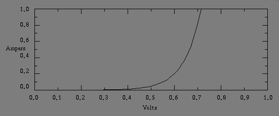
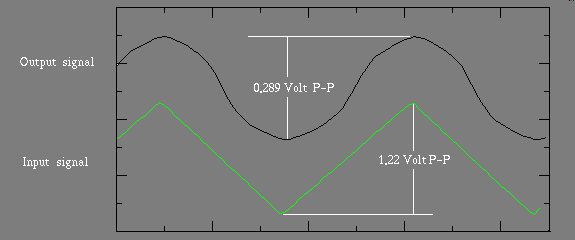
In this range the diode is neither completely on, nor completely off. Its nonlinear characteristic is sometimes a problem for circuits we build, because nonlinearity introduces distortion into a signal path. On the other hand however that same nonlinearity, because it is exponential, or logarithmic, depending on which characteristic you reference, I.E. current, or voltage, with respect to the other, can be used to null out some other unavoidable exponential, or logarithmic distortion already present in your circuit. Not only that, because adding logarithms performs arithmetic multiplication, critically placed diodes in an amplifier circuit can produce an analog multiplier, or wave shaper. You can convert a triangle waveform into something approaching a sinusoid, by using a couple of diodes as a wave shaper. The following is such an experiment, I used the Velleman Oscilloscope to make measurements in the waveforms that follow.
Bipolar transistors:
In the simplest view, a transistor is nothing more than a current amplifier. If there is adequate voltage available, and of the right polarity, at the terminals of the emitter, and collector, the current that flows through the collector, will ignoring leakage, saturation, and a host of other details, be a preset multiple of current flowing through the emitter base region. That trait, the multiplication of current, is amplification, in this specific case current amplification, and in the jargon of electronic data books, this characteristic has a name, we call it Beta and its symbol is the greek letter Beta it looks somewhat like an upper case letter "B" with a descender. This characteristic, and its attendant symbol usually has a numerical value that falls between 25, and 300. I say usually, although single transistors have been made for very specialized applications, at a noticeably higher price with guaranteed minimum specified Betas in excess of 1000 they tend to be low power, and rather low voltage devices as well. On the opposite end of the spectrum, some specialized transistors optimized for very high emitter to collector voltage, tend to have Beta specifications as low as 7.0 and they are also more expensive. Another term you will encounter when talking about amplification, is Gain. In the case of Beta the Gain being referred to is specifically current gain. Two or more transistors wired up in a configuration called Darlington results in current gain that is the arithmetic product of both transistors Betas. For example, two transistors, with modest beta gains of 70, and 75 wired up into a darlington pair configuration results in what appears to be a single transistor with a beta gain of 5250. Manufacturers sell devices called Darlington transistors wired up this way, and sealed inside a single three lead plastic case. Using one of these saves you the effort of wiring two transistors up in such a configuration. It is not unusual to see darlington pair devices with betas in the tens of thousands. It's not without a downside, since there are two emitter base junctions effectively wired in series, the forward bias voltage of a darlington pair is twice the forward junction drop of a single transistor, and as an engineer you must take this into consideration, when designing circuits based on these devices. Plane old transistors, the kind you think of then you think of a non exotic device, are called bipolar transistors. They are a device with two junctions, placed very, very close to each other in an otherwise unremarkable block of pure intrinsic Silicon. The doping is set up to go from "P" to "N" and back to "P" again or they can be made the other polarity where the doping goes from "N" to "P" and back to "N" again. Some things that influence the design of the doping concentration are that to have a useful transistor you want reasonably high beta and you would also like to have as high an operating voltage as possible. As I have pointed out to you these two characteristics are at odds with each other. The most common types of transistors strike a balance between these, and other tradeoffs. Across the spectrum of transistor types that you find in the data books, the tradeoffs I will teach you will as you read the specifications almost jump right off the page, and when you see a device that seems to violate the tradeoff mentality, it seems to have the best of all worlds, you had better be suspicious of the one characteristic that seldom finds its way into a data book... The price!
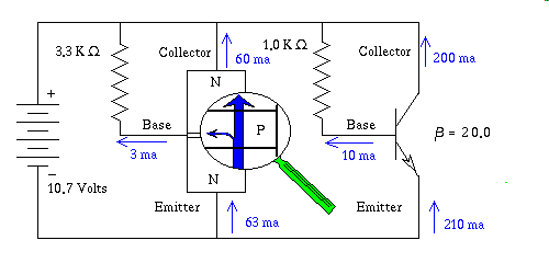
Ok enough already, here's a drawing of a biased "NPN" transistor.
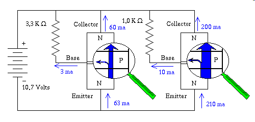
I show the electron paths in blue, by the way electrons are blue regardless what you may have heard about them being some other color :-) They leave the battery at its negative terminal, travel through the circuit and ultimately arrive at the positive return battery terminal. I simultaneously show two instances of either the same transistor, or if you prefer, two separate, but absolutely identical transistors. However you view it I am illustrating only one transistor here, so that I can show the effect of two different levels of base bias in a side by side comparison. The Beta gain of this transistor is 20.0 the junction drop is 0.7 volts exactly. The transistor on the left has 3 milliamperes of current flowing through its base, and this causes 60 milliamperes to flow through its collector, the 3 ma is arithmetically multiplied by the Beta factor, and this results in the 60 ma collector current. If you were to open the 3.3 K Ohm resistor, or short the base lead to the negative battery terminal, the base current would stop, and since the collector current is dependent on base current, the collector current would also cease.
What is happening here:
In the above drawing the electrons flowing into the Emitter terminal have at first only one path of current available to them. They flow across the Emitter Base junction into the base region by forward biasing what first appears to be a diode. Since the Base Collector junction from this vantage point represents a reverse biased diode jumping that gap is very unlikely, instead what happens is those electrons exit the Base lead wire, traverse the resistor, and return to the battery's positive terminal. This activity sets up a condition that is regularly replenishing charge carriers in the Base region. Due to the Base region being made very thin, and very wide, and deep comparatively speaking, having such a large number of charge carriers bouncing around in such a thin region, it becomes far more likely that they will diffuse into the Collector region, than travel down the long thin plane edgewise to make it to the Base lead wire. Therefore the thinner, and wider, and deeper you make the Base region, the higher the Beta gain the device will have.
If you turn on, Base current, Beta times that amount of current can potentially flow through the Collector. If you wire up a circuit that limits the current that is allowed to flow through the Collector to a point below the Base current multiplied by the Beta gain, the transistor is said to be saturated. When a transistor is in saturation it exhibits an unusually low voltage between the Emitter and Collector in fact a transistor so biased can exhibit Emitter-Collector voltage considerably below the forward bias voltage. This may seem to some of you to defy logic. How could you possibly have a Emitter-Collector voltage lower than the forward bias junction voltage. It would seem that for electrons to get through the first junction, on their way to the second junction there would have to be at least 0.7 volts to account for the Emitter-Base junction, since it is in series with the crystal region that holds the collector. The way I explain this, is that we are concerned only about charge carriers migrating through the crystal. While it is true that it requires 0.7 volts to free charge carriers to move within the crystal, once they are in motion the current they can carry, is carried from the Emitter to the Collector if they don't exit the Base lead first. They can and do drive the Collector below the voltage of the Base with respect to the Emitter. This is a charge phenomenon, in fact the Base-Collector junction is still reverse biased, even though current flows into the Collector. If you turn on, and off the Base current, in a transistor that has a current limited Collector such that Saturation is certain the transistor's output voltage, measured from circuit ground, where the Emitter is wired as the ground, or reference terminal, with the output voltage measured at the Collector, the output will go from one extreme, the transistor full on, and virtually zero volts at the Collector, to the condition called cutoff, eg. the transistor turned as far off as possible, meaning no current flows, and the voltage measured at the Collector being nearly the voltage of the power source. This action has been seen by some, to warrant calling the transistor a controlled switch, in that it can switch current on or off. My feeling is that such an explanation is an over simplification.
In truth there is no such thing as "digital" in the real world. All sources of naturally occurring information originate as an analog signal, we merely choose to represent this information as parallel digital data out of necessity, or convenience, in an effort to escape the noise of the analog world. Indeed the very circuit blocks we build that we call digital are composed of analog components, and if not operated within the tightly specified constraints the manufacturers lay out in the data books, and app notes; these so-called "digital" devices show there true analog nature. I'll give you one example. Some types of CMOS logic specify that a logic one must never be below a specified voltage, about 2.5 volts, and they also specify that a logic zero must never be above 0.8 volts. Obviously to transition from a one to a zero, or vice versa, you must violate this rule. So they make an exception to this rule, by telling you in the data books that you must accomplish this within a very short period of time, usually in the nanosecond range. Guess what happens if you deliberately violate this rule. The device goes analog, producing output voltage that is an analog voltage between a logic one and a logic zero on average, and it tends to oscillate at very high frequency, higher than the device is designed to withstand, and left in this state for very long often results in the device self destructing, from overheating a tiny portion of the silicon chip. Further if you look closely at the circuitry inside the chip you see a very serious problem with placing on an input any voltage between the permitted ranges for a logic one, or zero. The totem pole output transistors, MOS-Fets in this case, both turn on simultaneously, creating an electrical short circuit directly across the powersupply! No wonder it self destructs. To understand anything in electronics, even digital, you need to know how devices behave in the analog realm. Please heed this warning, you will be insufficiently prepared to deal with the digital realm, if you forgo the effort to adequately understand the analog realm. I have seen people attempt this, thinking that if they simply read the guidelines in the data books, and app notes, that's all they will ever need. Then when they try to design a digital circuit of a challenging complexity things go horribly wrong. The circuit misbehaves in ways they have no hope of understanding.
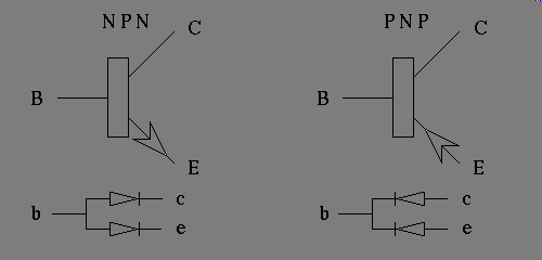
The transistor in question is an "NPN" that piece of information is encoded into the symbol by the direction the Emitter arrow faces. If it had faced pointing toward the body of the transistor, that is the vertical line which represents the silicon wafer, it would instead denote a "PNP" device. To help you keep straight in your mind which is which, imagine the arrow having a perpendicular line attached to the point of the arrow. This would form the symbol for a diode, and that will indicate to you what polarity the Emitter Base junction is, for both forward and reverse bias.
If you only connect two terminals of a transistor at any one time, not a very useful configuration, it will behave as if it were two diodes. Since your ohm meter has only two lead wires with which to connect a component to, simply leaving the third transistor lead wire dangling in the open air, and connecting the leads of the ohm meter to any two lead wires of a transistor, allows you to observe the two diode junctions formed inside the transistor. The transistor is of course a far more interesting device than this simple exercise lets on, but it is useful for both determining whither the device is an "NPN" or a "PNP", and it clearly identifies which lead wire of the transistor is the base lead. This information, in the absents of any real documentation on the part, or even worse, in the case where the transistor in question is House marked, that is stamped with a number that has meaning only within the confines of the factory that produced it; may indeed be the only way you can figure out anything at all about the device.
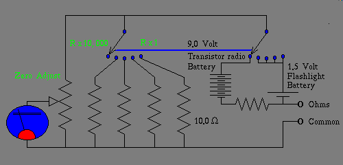
Using a simple electro mechanical ohm meter, that derives its power from a single 1.5 volt flashlight battery, a silicon junction drop appears to be approximately half scale, regardless what ohms range you set the meter to. This is not strictly true, but it tends to be more true, than behaving like a resistance. The reason this happens is because the 0.7 volt junction drop, is almost half the voltage of the flashlight battery inside the meter. The reason it is not strictly true is that the diode junction drop is as I've pointed out before a natural logarithmic curve of the current, and the ohm meters short circuit current of each successive range multiplier is a factor of ten different from the adjacent setting. The point of all of this, is that you can read the junction drop of a diode or transistor, directly off the dial, by using a linear range, such as a voltage scale, and multiplying by a fixed constant, if your particular meter lacks a 1.5 volt range, and then subtracting your adjusted reading from the fullscale value, namely 1.5 volts. Because the meter selector dial for the ohms ranges offers up currents a factor of ten apart, if you know the fullscale current of any one of them, you simply multiply by factors of ten to get the others. If you know the fullscale current, for a given range, if you multiply the percentage of the present needles deflection, times the known full scale current, you can get the current that is flowing through the diode under test. Without even turning the meter on, by simply knowing that it is powered by a single 1.5 volt flashlight battery, and picking a spot about half way in the middle of the dial, looking for a point where both a resistance, and a voltage intersect you can compute by using simple ratios the fullscale current, for any range available to the selector switch. This unusual application of a simple VOM, Volt Ohm Milliammeter thus makes possible a poor mans Diode curve tracer, and two such meters, applied in this fashion, allow you to accomplish what a Transistor curve tracer does. This may seem like a lot of mental gyrations to save a mere $3000.00 but consider that Transistor curve tracers are heavy pieces of electronic gear, and working in the field, you are often making repairs while standing on rickety scaffolding, that getting a heavy fancy curve tracer up there to make one measurement might make you envious of the guy who really knows how to make good use of the simpler, and lighter, piece of gear.
In the above exercise I show using a simple ohm meter, to measure diode voltage to current relationships. I show you how to take the short circuit current directly off the dial mathematically. You might ask why not simply use another meter to measure it. If you derive this value mathematically, and measure it, the two will not agree. My method is not at fault here, your use of the second meter is. Why? Because the second meter, set to measure current, drops a quarter of a volt at full scale. Since we only have 1.5 volts to work with, that quarter of a volt is a significant error.
In my case I have a Micronta Range Doubler 22-204C multimeter that uses a 1.5 volt flashlight battery for all but the highest resistance range that being the R x 10,000 range, which uses a 9 volt transistor radio battery. So for this experiment I will use the R x 1 -to- 1000 ranges inclusively. The meter dial itself sports a scale intended for use with both voltage, and current that spans zero to ten. This is convenient, as it permits me to use this linear scale, as a decimal fraction, or percent scale. Reading a 1N4001 rectifier diode, these are rated at 1.0 amp RMS, so even the fullscale current of the R x 1 scale is well within the safe operating range of the diode. Upon measuring the diode on the ranges that are powered by the 1.5 volt battery. The following decimal fraction values come to light.
0.50 read on R x 1
0.59 read on R x 10
0.64 read on R x 100
0.72 read on R x 1000
To make them useful we must arithmetically convert the reading to voltage across the diode, and current passing through it, using the following formula.
E = (1 - Scl) * 1.5

I = (1 - Scl) * RngCur

Where:

E      = Voltage across the diode

I      = Current through the diode

Scl    = the decimal fraction read off the dial

1.5    = full scale meter voltage, eg. the battery

RngCur = full scale meter current, for a given range.

Applying this bit of arithmetic treachery, yields...

Rx1    diode Volts = 0.75     = (1 - 0.50) * 1.5
Rx1    diode Amps  = 0.075    = (1 - 0.50) * 0.150

Rx10   diode Volts = 0.615    = (1 - 0.59) * 1.5
Rx10   diode Amps  = 0.00615  = (1 - 0.59) * 0.015

Rx100  diode Volts = 0.54     = (1 - 0.64) * 1.5
Rx100  diode Amps  = 0.00054  = (1 - 0.64) * 0.0015

Rx1000 diode Volts = 0.42     = (1 - 0.72) * 1.5
Rx1000 diode Amps  = 0.000042 = (1 - 0.72) * 0.00015

     +----------------------------------------------
     |                                            *
0.07 |                                           .
0.06 |                                          .
0.05 |                                         .
0.04 |                                        .
0.03 |                                       .
0.02 |                                     .
0.01 |                                  . *
0.00 +------------------------*------*--------------
    0.0   0.1   0.2   0.3   0.4   0.5   0.6   0.7

The plot above is Current on the vertical axis, and
Voltage on the horizontal axis, of the above data.

Asterisks "*" are actual measurements, dots "." are
my crude interpolation attempt using ASCII art
Notice that we are not reading the ohm scale of the meter to get this
information, in spite of the fact that we are using the ohms range selector
switch positions to actually subject the diode to mild voltage, and current
stresses that give us information about the diode's forward bias
characteristics. The thing that permits us to do this is that we are
applying an understanding of how a multimeter works, to a task it was
never intended for, but is nonetheless useful, and reliable. You can just
as easily apply this technique to a transistor by forward biasing its
Emitter Base junction with one ohm meter, while using another
ohm meter to observe the Voltage / Current relationship of the
Emitter Collector terminals. The beauty of this is that you
don't even require a bench supply to perform such a test.There are of course fancy digital multimeters that will measure a transistors beta gain. They have built right into the front panel, a cute eight pin socket that you plug in the transistor to be tested into three of the holes in the socket. The choice of which holes you use, hinges on whither the transistor is of type "NPN" or "PNP", and what the order of the Emitter / Base / Collector orientation is. I'm not arguing against the purchase of such a device, just that you probably don't want to rely on it. Using my simple ohm meter approach offers you one really big advantage they don't provide. You can not only measure the beta gain, but you can do so at, in this example, four different current settings. If you are measuring beta, it's important to do that measurement at a current that is near the actual current you will be subjecting the device to, when you wire up your circuit. This is because the beta is somewhat current dependent.
Since transistors amplify current, the voltage that is present between the Emitter, and Collector has little to do with the current flowing through the Collector this behavior is not at all like a resistor, whose current is linearly voltage dependent. There is a thermal effect though, but it can be nulled out with feedback. This is truly something new, something that you haven't seen before, a device that within a voltage range acts as a circuit element to limit current irrespective of the voltage across it. It is within these limits a constant current source a thing quite different from a constant voltage source. The current it controls as I have said is a function of Base Emitter current, and the beta gain of the transistor. So what are these voltage limits I am so carefully constraining this system to? The lower limit is that you must be dropping enough Emitter Collector voltage that the transistor is not in Saturation. Not even the onset of saturation. Since saturation is lower than the junction voltage, by a few tenths of a volt, a good rule of thumb is keep at least seven tenths of a volt across the Emitter Collector terminals if you want the transistor to act as a current limiter. At the high end the transistor will avalanche if the Emitter Collector voltage is too great, the avalanche voltage is considerably greater than the posted specification sheet for the transistor, by its manufacturer, so simply staying below the absolute maximum rating given you by the manufacturer will be one limit at the high end. Another limit is thermal dissipation of the transistor's package. If you draw 20 ma through the Base of a transistor, whose Beta Gain is 20, the Collector current will be 400 ma. If across that same transistor's Emitter Collector terminals you are dropping 40 volts the transistor is dissipating sixteen watts of heat! You can melt solder on a package the size of a transistor dissipating that much heat. There are several ways to deal with this, Heat sinks, these are metal finned heat radiators that help spread the heat into the surrounding air, Fans, do a much better job of this, and in extreme cases Water Cooling systems, not very different from the ones in your Car's Radiator. This all goes back to earlier lessons where I got rather "preachy" about watts. Basically you are multiplying the Voltage, in this case across the Emitter Collector connection, by the current flowing through the Collector it's as simple as that. So now the mystery of the limits of voltage min and max is solved. As long as you stay inside these extremes the Collector will faithfully represent Beta times the Base current, assuming of course you have the polarities right.
Because of a resistors linear voltage to current relationship the more current you draw through a resistor, the more voltage it drops. If you place a resistor in series with the collector of a transistor that is controlling collector current via beta, times the base current, the voltage drop across that resistor is now proportional to the collector current. The following is an important heads up, don't forget this, or you will be very confused. The resistor is connected between the powersupply and the Collector since most measurements are relative to circuit ground the affected point, the point where the collector, and resistor come together exhibits a decreasing voltage with respect to an increasing current. This does not mean the resistor is working backwards, if you were to measure the voltage drop across the resistor itself, that voltage does behave as you would expect. However in a practical observation, the meter has the common terminal connected to the same circuit ground that all the other equipment is ground referenced to. This is necessary equipment technique, because as more and more pieces of equipment are connected to a circuit, if the grounds are connected to arbitrary points in the circuit electrical safety grounds tend to short things out, and those pieces of non-grounded equipment can introduce confusing noise signals into sufficiently high impedance circuits, that make reliable observations impossible. In addition to these reasons, circuit blocks are typically connected to each other sharing a common ground. So you as an engineer have to make these transformations anyway. They take a little getting used to, but after a while they come quite naturally. This characteristic, of exhibiting a decreasing voltage at the collector, while the base current is increasing or vice-versa, has a name, we call it inversion, and it is crucial to many facets of electronics, things such as oscillators, and the most fundamental gate in a computer, a thing called an inverter, would not be possible if inversion were not possible.
Inversion:
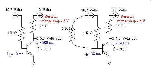
In the left diagram in the above schematic the base current is limited by a single 1000 ohm resistor that is fed by a powersupply that is ten volts above the junction drop of approximately 0.7 volts. I label this supply as 10.7 volts. This insures the base resistor has approximately 10.0 volts across it. Thus to compute the base current is simple ohms law, ten volts divided by the base resistors resistance. Once the base current is known, with a known beta gain factor we can compute the collector current by multiplying the two. Once the collector current is known one simply multiplies that by the resistance of the collectors series resistor, again using ohms law, to get the voltage drop across the, in this example 25 ohm resistor. Then the final step is to subtract the collector resistors voltage drop from the collectors powersupply in this case conveniently set to exactly ten volts to give 5.0 volts at the output terminal.
In the right hand diagram we reach into our box of resistors and grab a 5000 ohm resistor, and bend its leads so that we can jumper it across the existing 1000 ohm base resistor, to temporarily increase the base current a little bit. This 5000 ohm resistor being added is the Independent Variable of our experiment, and it causes many effects. The final result, the Dependent Variable ultimately exhibits a lower output voltage at the collector.
The gist of where this is going is that here we are observing a phenomenon where an increase of input current, causes a reduction of output voltage. We call this inversion. Also true is the opposite side of the same coin, a reduction in input current, produces an increase in output voltage. This second statement is really no different from the first statement, in fact you can get the results from the first data set, to prove the second assertion by simply reversing the order in which each scenario is presented.
It is important to the study of electronics to truly understand this. The concepts developed here are used in circuits throughout the entire discipline. One of the concepts I have slipped into the mix with out mentioning it by name, is the idea of what exactly a pull-up resistor is. If you really didn't get what inversion is don't despair, my description of the concept of a pull-up resistor may bring it all home to you.
Pull Up:
If you were to open the base lead, thus stopping all current flowing in the base of the transistor, the collector current would also be similarly reduced. Zero base current multiplied by any fixed factor for beta gain produces zero collector current. Zero collector current means no voltage drop across the 25 ohm resistor. When the resulting voltage drop of zero is subtracted from the 10.0 volt powersupply, the output voltage at the point where the collector, and the 25 ohm resistor are joined, is also 10.0 volts. The resistor is said to have pulled up the collector to the same voltage as the powersupply. At the other extreme if you replace the 1000 ohm base resistor with a 100.0 ohm resistor your base current shoots up to 100 ma, and multiplying by a beta of 20.0 gives a collector current of 2.0 whole Amperes. The 10.0 volt supply limited by the 25 ohm resistor simply is not able to deliver any more than 400 ma, so the transistor is saturated, with about 0.2 volts between its collector and emitter. In this example it is said that the transistor is pulling down as hard as it can, against the pull-up resistor and has won the battle so completely, that the pull-up resistor never had a chance.
Another way to state this is to say that the transistor is loading down the current limiting collector resistor pulling its potential all the way down to the ground potential, or at least nearly so. In the previous case where we interrupted all current to the base, the 25 ohm resistor wins the battle, because the transistor is not loading down the 25 ohm current limited voltage at all so it is pulling up the collector all the way to the 10 volt supply. In the case where neither the pull up nor the collector of the transistor is completely winning or loosing, that is some state in between the two extremes, we call this the analog or linear range of operation, and a circuit that operates only at the two extremes is called digital or switchmode operation. A circuit that operates in both digital and analog at the same time, is called an analog circuit that is overdriven and there are examples of such devices sold commercially, one such device is the well known Guitar Fuzz box, and its variable filtered cousin the Waa-Waa Pedal.
All that I have told you in the preceding section is factual, but in the real world of discrete devices, not very practical. Integrated circuits are another matter entirely, they get away with doing things in IC design because the entire IC chip is so small that the whole thing runs at the same temperature, and the concentration of the doping compounds is uniform over the whole IC chip, again in part because it is so small. The realities of working with discretes, individual packaged transistors means several things. One transistor can by dissipating more watts than another component on the board, be running at a significantly different temperature than another. The realities of mass producing transistors often results in wide variations of beta gain from one lot to the next. If you read the databook, it is not uncommon to see the spread of min/max beta gains for a given transistor part number to vary by as much as 400 percent. Indeed often they don't even spec the max beta for "economy" transistors at all. What's an engineer to do. Well for one thing don't rely on beta, as a spec that you can nail down. A statement such as this probably seems ludicrous in light of how critical beta is to the operation of a circuit. The answer to this seeming inconsistency is that to build a practical and reliable circuit you need to introduce feedback to compensate for these wide variations in beta gain. If you design your circuit conservatively, not only will beta variations be brought under control, but some of your thermal instabilities will also be covered as well. The more conservative the design of a circuit, the more likely you are to be able to call out dozens of different transistor numbers, as substitutes for a device that may in the future be discontinued, no longer to be manufactured.
This section shows how to design simple conservative practical amplifiers that require no critical, low tolerance, I.E. high precision, eg. expensive components made of the element "unobtainium" :-)
This approach to design tends to make these circuits less vulnerable to wider temperature extremes as well. Wann'a design a circuit that goes into your automobile, you better think about the temperature extremes the cab of your car can reach. If you drive to northern climates, in winter, at night it is possible to experience temperatures below minus forty, and in the summer a closed locked cab in some southern states, can melt a vinyl LP record album so totally that is shrivels up into a ripely Christmas Tree ornament that most resembles a Starfish in shape.
Seriously, do you really expect your circuit to work under those conditions? Well GM, Ford, Chrysler, etc. do this sort of thing all the time. They test their circuits in environmental testing chambers. You have such equipment in your kitchen, namely the Refrigerator, and the Oven, Not the Microwave, the conventional Oven, ok. :-) Subjecting your circuit to the Microwave-Oven would be like testing to see if it would withstand the spearhead of a solar flair! Yikes! On the bench any source of heat or cooling can get you some preliminary results, a heat lamp, an Ice Cube, the hot tip of a soldering iron, or Freeze Spray sold in electronic parts shops for tracing thermally intermittent components, can give you some idea how things will act, but nothing beats the tried and true conventional Oven set to 150 degrees Fahrenheit, and then to test the other extreme the Freezer section of your Refrigerator. When doing the last test, beware of moisture condensation, a sealed cabinet with a new or re-cycled Silica Gel packet generally eliminates this problem. I have heard, but not yet myself confirmed the efficacy of a technique of "baking" used Silica Gel Packets to restore their Hygroscopic properties. Incidentally if you don't know what Silica Gel Packets are, you've probably thrown away a dozen or so of these things. They are the little packets that come shipped with nearly every electronic device you buy, the only instructions on the packet is a short message that says "Don't Eat" I never eaten one of these so I'm not qualified to tell you what they taste like. They do however aggressively absorb water vapor, and inside a sealed container they dry out the air inside. Their mortal enemy is the humidifier, so they tend to loose their effectiveness if left out in the normal room air. For completeness sake I should mention simulators, such as Spice. Simulators can if you don't make any mistakes, and if you don't accidentally exceed the mathematical precision of a Spice library, accurately predict what your circuit will do at various temperature extremes. Relying on these software tools to tell you if you missed anything is one thing, trying to use them to tweak your circuit will lead to irrational, and inaccurate conclusions, because you are much more likely to exceed known limits of precision in a given library without realizing it. They are indispensable tools for IC design, but not that useful for discreet component circuits. The problem is that you cannot rely on one vendors Spice Library to be a perfect fit to another manufacturers component, and since design using only one manufacturers product line in any large complex circuit is all but impossible, eg. they won't have a component you need, or they ask too much money for it, your Spice simulation is not likely to accurately represent any real circuit you build. On the bright side there is a GPL version of Spice for what that's worth. In my presentation I endeavor to show how to design a circuit conservatively enough that you can more easily cope with these parameters, because you have a wide range of tolerance to work within, without getting anywhere near the danger zone. Even if you find yourself approaching the danger zone, because you are "in the loop" you are keenly aware of the tradeoffs you were considering at that time. The simulation approach has the problem that you are not really designing the circuit, the computer is making countless decisions for you, some of which if you knew what they were you'd be horrified by the ghastly assumptions made on your behalf.
There are three basic configurations of the simple transistor amplifiers. One each, in which for each case, a single different transistor wire is held at some AC reference, eg. common, and the other two wires are used to amplify signal. These configurations are given names based on which of the three transistor leads are chosen as the AC ground reference, or common reference. Their names are as follows, common Emitter, common Collector, and perhaps somewhat less useful the common Base configuration. You are expected to build these, and given that I have designed them so that you are required to make as few changes as possible to transform one of these amplifiers into another. Since the circuit is conservatively designed none of the values are terribly critical, meaning if the nearest value of say a resistor is within fifteen percent your circuit will still work, just not as optimally as it would have if the proper component had been used. My first example is the common Emitter, and common Base, configurations shown side by side, they are remarkably similar.
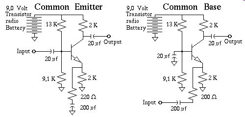
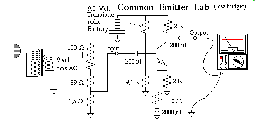
To discuss the AC paths of this circuit, for simplicity I will assume that the output is driving a load such as an oscilloscope fitted with a times ten probe, such that it's load is negligible, and that the input is being driven with a signal generator whose output impedance is so low as to be negligible, on the order of an ohm or maybe as much as two ohms. I will also stipulate that the frequency of the signal is between 400Hz and 10kHz to limit coupling losses in the capacitors to one percent. For example the 200 uf capacitor in the common base configuration at 400 Hz works out to less than two ohms.
                        1
1.9894   =  ---------------------------
            2 * Pi * 400 Hz * .000200 f
Since it's in series with a 200 ohm resistor the Xc introduces less than one percent of error. If you really want to do this as a lab, and you have only an AC wall-wart or Variac for a signal source, your signal source is by definition the frequency your Electrical Power Utility's output frequency. If you are in the US your line frequency is 60 Hz, elsewhere it varies but most everywhere other than the US the line frequency is 50 Hz. As a work around to allow you to use line frequency as a signal source, I suggest that you multiply all of the capacitor values by a factor of ten, so the 200 uf cap is replaced by a 2000 uf cap. and so on.
Ok let's examine the common emitter configuration from an AC perspective first. This is to be a second approximation examination. The emitter circuit is from an AC point of view a 2k and a 220 ohm in parallel from the emitter to ground the parallel equivalent resistance is 198 ohms, I choose to call it 200 ohm to make the figures easy. A 200 ohm emitter impedance to ground looks from the base lead perspective, after you factor in a beta gain of 20.0 like 4000 ohms. So to get the effective base loading using a trick borrowed from thevenin, the AC base circuit looks like a 13K, and a 9.1K, and the beta amplified emitter impedance of 4k all wired in parallel. The AC base is 2.29 K ohm. Now to examine the collector circuit. The collector itself looks like a current source, and believe it or not it has an infinite impedance. The only other component in the collector circuit that could possibly act as a load is the 2K ohm resistor. Since the AC component of input signal voltage is being duplicated at the emitter, and the emitter to ground impedance this voltage is impressed upon is 200 ohms, and since the impedance in the collector circuit is 2K ohms, and nineteen twentieths, of the actual current to drive the emitter impedance is in fact coming from the collector circuit, this circuit is a voltage amplifier with a voltage gain of nearly ten to one. For all practical purposes the gain of any conservatively designed common emitter amplifier is the ratio of the total collector impedance divided by the total emitter impedance.
     Collector impedance
Av = -------------------
     Emitter impedance
Where Av is an abbreviation for Amplification of Voltage. Without giving you a bunch of formulas, I have using ohms law, and a few other techniques, shown you how to derive all of this on your own. If you study this section carefully, you can begin to design amplifiers of different gain factors, and input/output impedances to suit your needs as they arise. Since this amplifier has a voltage gain of ten, and can at most produce an output signal of 3.0 volts peak, you require an input signal of 0.3 volts peak applied to the input to fully drive the amplifier. If for example you were considering using an AC Wall-Wart whose output RMS voltage was 9.0 volts AC an attenuator would need to be constructed to reduce the 9.0 volt RMS output to 0.3 volts peak. May I suggest using a 1.5 ohm resistor in series with a 62 ohm resistor wired across the Wall-Wart, and using the voltage dropped across the 1.5 ohm as the signal source to connect to the input of your amplifier. Note: These values do take into account the RMS vs peak voltages involved. Better yet, use three, use a 1.5 ohm, and a 39 ohm, and a 100 ohm rheostat, eg. variable resistor, all wired in series, this will give you a knob that you can turn to adjust the input signal over a fairly wide range.
Common Base:
As in the common emitter the AC impedance ratio of the collector to the emitter circuit is for the most part what controls voltage gain of the transistor amplifier itself, however inherent in the design of the common base configuration is the fact that the emitter AC impedance reducing circuit used to set the AC voltage gain now also forms a voltage divider that attenuates the input signal before it reaches the emitter. Both of these configurations have an AC voltage gain of ten, but if you look closely at the AC paths from the emitter to ground, the gain limiting resistor in the common emitter configuration is 220 ohms and in the common base it's only 200 ohms. This causes the common emitter amplifier to have a gain of ten as the emitter impedance is 200 ohms when the 2K ohm resistor is considered, on the other hand the emitter impedance through the generator, remember I called out a very low impedance generator 1.5 ohms, so that the generator's impedance could be ignored. Thus the combined emitter impedance of the common base is only 181 ohms, and the works out to a voltage gain of eleven to one, within the transistor section itself, however, the 200 ohm resistor in series with the generator and emitter, through a negligible 2000 uf cap. creates a 10 to 11 voltage divider. When you multiply the ratios of the front end attenuation, by the emitter/collector voltage gain, you get exactly ten.
              Terms
            /       \
     Attenuation   Amplification

        2000          2000
10  =   ----    *     ----
        2200           181
It is important to mention that the base is an AC short to ground
in this common base configuration. The capacitor between the base and ground
essentially insures that the base is not free to move in voltage at the
whim of the emitter activity reduced by beta.
So if the ratio of Collector to Emitter impedance is what controls the AC voltage gain, what if we create an AC short from the emitter to ground, couldn't we expect a nearly infinite voltage gain? If you did this the gain would in fact be very high, but it would also be unpredictable. For instance in a common emitter circuit, with a voltage gain of ten the effect of the transistor's beta gain on the input impedance has little impact. For example an emitter impedance of 200 ohm multiplied by an unusually low beta of 20.0 appears to the base as 4000 ohms, significant, but not serious. To ask for a voltage gain of 100 would require an AC emitter impedance of 20 ohms, and once again multiplying that by a beta of 20.0 again still our worst case scenario works out to a 400 ohm AC base loading effect. The total input impedance of our amplifier with a voltage gain of 100 is now only 372 ohms. If it were being driven by a previous stage with no load a voltage gain of 10 and and as in our example a no load collector impedance of 2000 ohms, this 372 ohm load when factored in reduces the gain of the previous stage to 1.57 hardly any gain at all. Remember Unity Gain a gain of 1.0 is is the gain of a simple wire, no amplification, and any body trying to sell you an amplifier with a gain of less than one, is in fact selling you an attenuator, a device that reduces the signal, rather than amplifying it.
All of engineering is mired in the art of managing tradeoffs. Aggressive design presses you ever closer to the point where ever more factors must be considered, to make a system work reliably over the varying conditions, and manufactureable over time, and across vendors. Reducing emitter impedance to set the gain higher you must begin to consider the internal spreading resistance of the base region of the transistor itself, and the larger factor, because it is not being amplified by beta gain, the internal emitter base forward junction effective resistance, which is not really a resistance at all, it is instead similar to the diode current, to voltage curve, and for very small excursions of voltage, behaves somewhat like resistance. These things have names R'b, and R'e while we strive to make them as insignificant as possible using conservative design they do affect the AC performance of our circuits, as you will see. R'e is given by
             vT
R'e  =     ------
             Ie
Where:
R'e =  effective internal
       emitter resistance

vT  =  Thermal voltage
       approx 25 mv at
       room temperature

Ie  =  Current flowing
       through the emitter
I covered thermal voltage vT earlier this section, it is equal to
Boltzmann's entropy constant k times the temperature in
degrees Kelvin T, divided by the charge q of
a single electron in coulombs, sometimes referred to in physics as a constant
named Elementary charge. At room
temperature, vT is approximately 25 millivolts.Two important things to note:
First understand that R'e is current dependent. This fact means two things, (1.) R'e changes depending on what circuit you place the transistor into, and (2.) R'e changes a little bit as the ebb, and flow of the AC signal goes through the amplifier. This means that the amplifiers voltage gain is changing slightly with respect to the instantaneous voltage seen at the base lead relative to ground. The higher the base DC voltage the more AC voltage gain, the lower the less. This is Logarithmic Distortion and it is a major contributor to something called Total Harmonic Distortion, sometimes abbreviated THD by the HiFi audio industry, and often cited by "Golden Ear" Audiophiles as the top of their list of things to minimize, and, or avoid. The way you keep this type of distortion to a minimum, is to avoid allowing R'e to be a major component of your voltage gain. In other words, keep the gain reasonable, and use conservative design criteria. Add an extra stage if you need more gain.
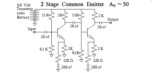
The second thing to note, is that if a single stage common emitter, amp results in inversion, what happens if you cascade two of them together, that is, what do you get when you invert the previously inverted signal? You get a normal, non-inverted signal. Three common emitter amplifiers chained together result in an inverted signal again, and so on. Basically an odd number of common emitter amplifiers, ends up inverted, and an even number makes a non-inverted output. Note that I was careful to specify common emitter amplifiers when talking about inversion. Common base, and common collector amplifiers do not invert the signal!
Running the numbers of R'e on this simple two stage amplifier from the quiescent point to near saturation, and then plugging the R'e variance back into the gain equation you get about 4.7 percent distortion, which is pretty bad, but when the signal hits the second stage, it too distorts the signal, but because of inversion the logarithmic nonuniformity is for the most part nulled out. If you were to exaggerate this logarithmic distortion, of just the first amplifier alone, and look at it on an oscilloscope, what you would see is an output waveform whose top part of the wave was smashed down a little, and the bottom, or negative tips of the wave were elongated somewhat. Now flip that image upside down, and distort the result again exactly the same way, and it's obvious why this is so, the elongated peaks are now on top, so they get smashed, back toward their normal shape, and the smashed ones now on the bottom, get stretched out a little, again back to their normal shape as they go through the second stage of amplification. If you worked very hard to keep the voltage gain in any pair of stages of amplification as closely matched as possible, and the emitter currents are also matched Logarithmic Distortion can be held to tiny fractions of a percent. Golden Ears love this approach, they don't trust negative feedback, or at least that is what they tell you, what's funny about this, is that the external emitter impedance is in reality providing negative feedback. They, or at least many of them refuse to see it that way. I know I've probably offended an audiophile or two, please send your flames to dev/null I am endeavoring to explain this subject, to people who wouldn't understand the higher math anyway, if they are curious, and I'm sure some of them will be by reading this tirade, when they reach the point in their learning curve that they can comprehend the theory I'm quite certain that they will be vital members of the audio news groups.
In the above two stage common emitter amplifier I did not attempt to match these gain factors, because to match them you must take into account the output loading of the final stage amplifier, and since I am specifying it is not loaded balancing this, for minimum distortion is pointless. The input stage on the left, when the input loading effect is factored in from the stage on the right is the AC parallel combination of the left transistors collector resistor, 2K ohm, the two base resistors on the right hand transistor 13K ohm, and 9.1k ohm, and the effective right hand transistor's emitter to ground AC impedance, of 200 ohm multiplied by a beta gain of 20.0 worst case, gives us 4K ohm. This comes to 1.0674K ohm. Dividing that by the left transistor's emitter to ground AC impedance of 200 ohms gives a total AC voltage gain of 5.3372, and since the output circuit of the right hand transistor is open circuit, its gain is given by 2K ohm divided by 200 ohm, eg. 10.0 so total system voltage gain, of both stages of amplification is the arithmetic product of each individual stage. Thus 5.3372 times 10.0 is 53 or approximately Av = 50 for nice round numbers, absolute worst case.
I show how I got the numbers I got, so that if you are fuzzy on any of the details you can run the numbers yourself, and hopefully get the same numbers. Attempting to do this, and failing to get the numbers to come out right, probably means you, or I, goofed somewhere. If you think I goofed, you can always E-mail me, but E-mail once sent, is exceedingly difficult to withdraw, and if in fact you goofed, and then subsequently discover your mistake, you are powerless to pull back E-mail that will reflect badly on you. What I am trying to say here is that there is no such thing as a stupid question, just some that are more difficult to live down. :-)
So far I have discussed the common emitter, in depth, and given some coverage of the common base, I will cover more practical uses for the common base later in this course, but the one thing of the basic three configurations that I haven't discussed is the Common Collector circuit. The Common Collector circuit, is better known throughout the industry as the Emitter Follower, because it more aptly describes what this circuit does. Remember my saying at the outset, that bipolar junction transistors are in reality nothing more than current amplification devices. An Emitter Follower takes advantage of this by reproducing at the emitter a voltage slightly behind the input base voltage, but at substantially lower input base current than the emitter is capably driving the output load. The bulk of the energy to drive the load is emanating from a power source that is connected to the collector, however the signal characteristics of the base voltage, less the junction drop, are what is manifest at the emitter, albeit at much greater current; again the current is coming from the collector powersupply. What I mean by signal characteristics of the base voltage, is things like regulation, line ripple, or some intentionally injected AC signal voltage.
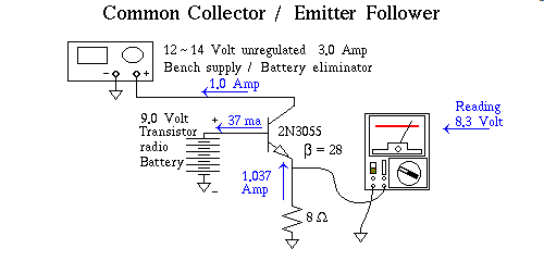
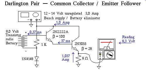
Still the nine volt battery is wasting away, at a 37 milliampere rate. We can minimize this quite a bit by adding another transistor, although we do suffer an additional junction drop, for the new, additional transistor.
The following circuit is your first serious electronic project. It is a regulated variable DC powersupply. You will use this device as long as you work with electronics. Even if you buy new, or design and build better better ones, an old working variable powersupply never lies idle, they do get used. You can never have enough of these gizmos, you will find yourself series them, using one for biasing, while the other one is providing main power, I even quick charge NiCad batteries on a bench supply rather than wait for them to charge in the charger, which can take days.
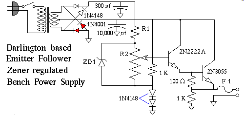
Let me begin this section by saying the best way to learn engineering is by doing it. The most important specification of any component is a characteristic called price. While some characteristics fluctuate with environmental conditions such a temperature, or vary widely from one lot number to the next, those things can be scientifically addressed by statistical analysis. The parameter Price however is a characteristic largely dependent on a myriad of market conditions, such as Supply, Demand, not to mention deliberate market manipulation, and since it is not an electrical characteristic, that directly affects the operation of the circuit, or system it is placed into, this critical parameter, is often not available in data books. Be that as it may, you as an engineer must consider this parameter when you design a circuit, for your design to be complete. A good first level approximation that takes into account the all important Price coefficient, involves looking at the system as a whole, looking for a single component that is noticeably more expensive than all the others combined. In this bench powersupply, that component is probably the power transformer. If you happen to have a suitable transformer on hand, or if you can find an inexpensive one at a surplus electronics store, that will fill your needs, at one tenth the cost of a new one, unless you are independently wealthy, the effort spent making that transformer work, is less of an effort, than the effort you spend in your day job, to earn enough money to buy the expensive new one. As I started this paragraph; you learn by doing, if you go out and buy a transformer, that does not require you to redesign the circuit given above, you may as well be building a predesigned kit, from the point of view of how much you are likely to learn. In lesson 014 about two thirds of the way down I give some tips on using an existing transformer that you salvaged from some other device, for use your project. I gave information on deliberately, and safely setting the taps of a transformer Wrong to make it produce a lower, or higher voltage than it was originally intended for. I then introduced you to a myriad of diode and capacitor configurations, that make possible the production of the desired DC voltage in spite of the situation not being perfectly suited to your project. I do not intend you to build this bench supply exactly as shown, you are expected to save money by redesigning it, a little, here and there, using what you already know. What you do need to know before you go off scrounging up a transformer, is what the requirements of the raw DC powersupplies are.
The Main supply:
This is the raw supply filtered by the 10,000 uf capacitor. It powers both transistors, and the 1K ohm pull up resistor that drives the two 1N4148 forward junction compensation diodes at the right middle bottom of the diagram above. This main supply is responsible for generating the output current of the entire bench supply. If the transformer after rectification, and filtering is only capable of delivering one ampere of current then that is the limit of your bench supply, and you should fuse it no higher than one ampere. However the 2N3055 power transistor is an awesome transistor, that can cost as little as $1.50 US ordered form the likes of Mouser, Digikey, etal. Here's what I mean by awesome, Power Dissipation 115 Watts derated linearly to 200 deg C, at a rate of 0.66 Watts per Centigrade degree. Maximum collector current of 15 Amperes Wow! and collector emitter breakdown voltage of a whopping 70 volts, when a 100 ohm resistor is placed across the emitter, and base, as I have done in my design. Note in order to take advantage of this voltage you cannot use the 2N2222A it breaks down at 40 volts, if you want to build the high voltage version of this supply, I give you an alternative transistor to use in place of the 2N2222A. The 2N3036 is an 80 volt transistor, with only half the beta of the 2N2222A, but the higher voltage bench supply is not going to as as capable in its output current because of may factors, chief among them power dissipation in the 2N3055 itself. At 60 volts across the emitter, and collector of a power transistor A mere 500 milliampere load will produce 30 watts of waste heat in the power transistor, and a simple two cell flashlight bulb, a number PR2 draws that much current. The compromise that one usually makes when building the higher voltage version of this powersupply is in the area of output current. With less output current, the lower beta in that higher voltage alternative to 2N2222A is not really a problem, however power dissipation in the 2N3036 used to substitute the 2N2222A is likely to be a concern, you may even have to consider devising some way to heatsink the 2N3036 driver transistor.
Part    Absolute Maximum         Minimum - Maximum
Number  Breakdown voltage        Beta

2N2222A   Vce = 40 min     Hfe @ 150ma = 100 - 300
2N3036    Vce = 80 min     Hfe @ 150ma =  50 - 150
2N3055    Vce = 70 min     Hfe @ 4.0 A =  20 -  70
Look over your stock of used transformers, and see if any you already have
on hand are usable for this project, in the voltage range you want to work
with. I also need to mention that the low current raw powersupply, the one
that powers the zener diode regulator circuit, need not be built as I have
shown here, and if you notice how low current that section of the raw
supply is you probably picked up on the notion that this raw supply does
very little work. In fact all it has to do is provide a few milliamperes
through the zener diode current limiting resistor R1 to
bias the zener diode into regulation, at a voltage high enough to allow you
to dial in the entire usable range available in the main supply. The
only critical thing about the zener supply is that it be a high enough
voltage to do this even during a brown-out. Translation... The zener supply
should be at least 33% higher than the zener's breakdown voltage.
And the zener's breakdown voltage should be at least as high as the unloaded
main supply. If you were to find a 110 Volt AC transformer
with two secondaries, a high current main winding, and a low current small
winding that was about one third the voltage of the main winding. If the
main winding serves your needs for the main raw DC supply the
smaller one could be used to build a small "pony" supply, that you wire in
series with the main DC supply. This adds the low voltage to
the high voltage, and insures the zener bias supply requirement is met.
Don't crowd too close to the breakdown voltage of the transistors, if you
suspect that your unloaded peak voltage will be 38 volts, don't
press your luck, use the 80 volt driver transistor.Murphy's Law:
Anything that can go wrong, will go wrong.
If you fail to heed this warning, and you go ahead and build it using a 2N2222A transistor, as soon as you plug it everything will work fine for a few minutes, and the Air-Conditioner will click off, and your house current wall socket voltage will increase a few percent, suddenly your circuits main raw supply is now idling at 42 volts, and the 2N2222A is breaking down, leaking an erratic two or three volts into the output, even though the dial is turned all the way down. I would advise staying under the breakdown voltage by at least ten percent, to allow for small voltage surges, and other variations.
After you have decided what raw voltage you are going to shoot for, you must decide what what the top end of your dial will set the powersupply output to. If you set your Zener voltage, that is you order a zener diode part number that has the desired reverse breakdown characteristic voltage, to a voltage slightly above the raw supply, you will be able to dial in the full range, the raw supply can deliver. Doing this has the drawback that the top end of the available voltage, falls in and out of regulation at the 120 Hz ripple frequency, or for those of you in Europe, and elsewhere 100 Hz. If you set this Zener diode voltage a little lower you will reduce the chance that it will allow ripple into the output, but also limit the maximum usable output. Perhaps a nice compromise would be to give it the full range, and then paint a red-line on the dial.
Now that you have selected your zener diode you need to compute the value of R1, and R2, the knob. The most readily available zener diodes are 1 watt, and 400 milliwatt, I advise you to go for the 1 watt variety if at all possible. Knowing the breakdown voltage of the zener, and its wattage you can compute what current it will require to dissipate the full one watt. Once that is known, you can compute the resistance of R1 by applying that current to what is left of the raw zener supply after subtracting the zener voltage itself from the loop. Be sure when doing this to consider the unloaded peak voltage of the raw supply, because that is the condition the unit will idle at, eg. spend most of its life doing.
        Raw  -  Vz
R1  =  ------------
           Iz

Where:

Raw = Raw Zener supply

Vz  = Zener diode rev-
      erse breakdown
      voltage

Iz  = 1 Watt / Vz
Ok I've just instructed you to bias the Zener diode to dissipate at its
absolute maximum dissipation spec, this hardly sounds like conservative
design rules, now does it. Well I'm not finished yet. Next you are going
to compute the value of R2. I want you to draw away from the zener
diode one third of the current, it otherwise would be converting to heat.
        Vz  *  3
R2  = ------------
            Iz
As a final step go back though all your calculations and use what you know
to calculate the wattages of resistors, and the highest possible voltages
that capacitors in your circuit are subjected to so that you may fully
specify all components of the system.One of the nice things about designing your own circuit, is that you are aware of all the tradeoffs you made in the design process. You go to the electronic parts store, and the part that you want is brand spanking new, and the proprietor of the electronic parts store is real proud of this one, you can tell he really likes this one, because he has priced it so high that only a five star General, somebody like General Dynamics :-) is the only person on the planet who could ever afford it. However sitting right beside it, is a prettier one, that would do the job, if you made minimal changes to your circuit... Yep, been there done that. Knowing how to engineer your own stuff has its advantages.
Here I give a practical version, using a real world transformer, and other parts. Let me see now, I'll just scrounge around in my box of medium sized transformers, here's one, it's a Radio Shack model 273-1512 by the way don't go out and try to buy one of these little gems, I seriously doubt they sell it any more, as it's pretty old. Its Primary is 120 volts at 60 Hz, and it has a single center tapped secondary winding rated 25.2 volts at 2 Amp this info is printed right on the outer layer of protective insulation. This means that if wired up as shown in the above circuit, the high current, main raw supply will reach
((25.2V / 2) * (Sqrt 2)) - 0.7V = 17.11if powered with 120 volts. However if we take into consideration that it is possible for the line voltage to be as high as 135 volts
((135 / 120) * (25.2V / 2) * (Sqrt 2)) - 0.7V = 19.35and the zener regulator circuit, the one that uses a 300 uf capacitor for a filter, will attain twice that much voltage 38.69 volts. Since this represents a fairly steep voltage rise on the part of the 300 uf capacitor I would add an in-rush limiting series resistor between the 1N4148 diodes and the capacitor, to limit the in-rush current just a little, to protect the 1N4148 diodes, since they can only withstand 500 ma for a one second surge an 82 ohm resistor will do the trick nicely. A 1N4747 zener diode breaks down at 20 volt, and is rated at 1 watt, so its max current is 50 ma,
      (38.69 raw peak) - (20.0 Vz)
R1  = ----------------------------
                  .050


      (20.0 Vz)  *  3
R2  = ---------------
           .050
Hence R1 = 390, note the actual calculated value
is 373.8 ohm, but you don't spec a value like that, because you
can't afford to buy it, I try to stay with 5% values and if a
choice has to be made between 360, and 390 ohm, the
higher value, is a lower current, so that is the safe choice. Plugging
the 390 ohm resistor back into the voltage across it, gives
us 0.89568 watts, so we spec that R1 is a one watt
resistor. R2 works out to be 1200 ohm, but try to find
a 1.2K ohm pot in your local Radio Shack,
however 1K is very close, and its lower resistance pulls even
more heat off from the zener, a good thing to do. If R2 is set
to 1K ohm it will dissipate 400 milliwatts, again
the nearest you will find is a one half watt potentiometer, so one half
watt is all you need, that said you could use a full one watt pot, and
you might consider this if you find the one watt pot to be easier to
mount, and find a mating knob for it's shaft, or find the one watt version
to be of superior mechanical construction, such as a metal shaft, versus
a plastic shaft. This potentiometer gets a real workout mechanically,
so spending a little more money on the front panel control knob makes
sense, especially considering you will likely use this powersupply for
many years to come.
Xfmr = 25.2 volt, @ 2 amp
ZD   = 1N4747
R1   = 390 ohm @ 1 Watt
R2   = 1K ohm pot @ 0.5 watt

Plus an 82 ohm 0.5 watt
in-rush diode protection res

Plus change the 1N4001 diodes
for a higher current diode
Forward current = 5.0 Amps
Reverse voltage = 50 Volts
Red Line:Where you place your Red Line is dependent on line voltage, and load current. An arbitrary choice of say 60% of the dial may not be the best way to handle this. Using the Radio Shack model 273-1512 for this example you should be able to achieve output current of 4.0 Amperes, assuming you changed out the 1N4001 diodes for a higher current diode, with useful output voltage of zero to twelve volts. Since the point on the dial at which ripple becomes a problem is mostly dependent on output load current, if you sample the this point experimentally at several currents, you end up with several places to put your Red Line mark on the dial. May I suggest that you place several Red Line marks, one for each current. This approach is useful, since you generally know in advance the approximate current your load will draw, you simply look at the appropriate Red Line mark for that current, and know that beyond that point regulation is no longer assured. I show below a test setup that will allow you to measure where the onset of ripple begins to interfere with regulation, using either a headphone, or the speaker out of a transistor radio, held to your ear so that you can detect the faint hint of ripple voltage riding on top of the DC voltage, that this test setup blocks from reaching the delicate headphone transducer element, by the judicious use of an AC coupling capacitor. I make some assumptions about the point in current which will elicit ripple from my experience in such matters, in short I pull the load numbers out of the air for the value of load resistors they are not all that critical, and you should measure the current and voltage, where you first detect ripple, for each Red Line you draw on the dial, number the Red Line mark on the dial itself and then make a chart, that you paste to the top of the instrument, that shows the red line, its current, and the still, but barely regulated voltage you measured, at that current. When completed you will have a bench supply that will allow you to push it right up to its very limit, and remain in regulation, and if you need more juice, you can push beyond this limit, albeit with loss of regulation, and clean DC filtration. Why might you want to forgo regulation? I'll answer that with a question, do you need pure regulated DC voltage to light up a light bulb, or run a motor, probably not, and you might really appreciate a little more power.
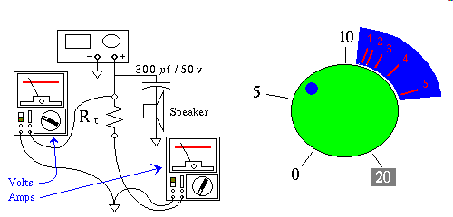
Mark   Load current   Load
nmbr                  resistor
 1     4.0   Amps     2.7  ohm  50 watt
 2     2.0   Amps     6.2  ohm  25 watt
 3     1.0   Amps     13   ohm  15 watt
 4     0.5   Amps     27   ohm   7 watt
 5     0.250 Amps     56   ohm   3 watt
In a pinch, you can use a resistor of inadequate wattage, for a short period
of time, if the spread between the required wattage, and the available
resistors wattage rating is not too great. The wider the spread the less
time you have to make your measurement, as every second that passes is
heating the resistor to higher, and higher temperatures. You can fan cool
a resistor, or simply blow on it. On occasion when testing computer
powersupplies that I repaired, the voltage was
low, 5, and 12 volts, I dug out an old coffee can, filled
it with water, hooked clip leads onto the resistors, and submerged
resistor and all in the water. This worked well enough that I was able to
run a lengthy burn in test, eg. many hours. However at the end of the test
the electro-chemical action of the water, made the resistor leads so brittle
that they broke off as soon as I handled them. So this is just a tip, not
a production technique. Also you might want to use a large high power
rheostat, (variable resistor) rather than guessing at where the two
intersecting lines cross, you can adjust the load as well to get currents
for your Red Line marks to represent exact currents. You will
see what I mean when you actually do this step. This is one those things
that is just too complicated to explain, but after you do it you will know
why I didn't attempt to explain it here.The right side of the above drawing is a mockup of what the dial will look like. If yours is not this fancy, after you have gotten the Red Lines marked with something crude like a felt tip pen, fire up Xpaint and make a nice front panel on your computer. If you are fortunate enough to have a Color Printer, color is a nice touch. They make full sheet sticky label stock, that will feed through your printer. Peel and stick, the label down to the front panel, and then add a layer of transparent laminating plastic over the top. Trim the excess, and presto, instant professional front panel. About the actual markings, 0, 5, and 10 volts are pretty obvious, 20 is shown in inverse video to indicate that this is only where 20 would be, but that the circuit cannot ever achieve 20 volts.